Gigabyte GA-7PESH1 Review: A Dual Processor Motherboard through a Scientist’s Eyes
by Ian Cutress on January 5, 2013 10:00 AM EST- Posted in
- Motherboards
- Gigabyte
- C602
Gigabyte GA-7PESH1 BIOS
As the server team at Gigabyte is essentially a different company to the consumer motherboard team, there is little cross talk and parity between the two. When the consumer motherboard side used the C606 server chipset for the Gigabyte X79S-UP5, the whole package got the consumer motherboard BIOS, software and utilities. With this C602 enabled GA-7PESH1, utilities such as the BIOS and software are designed in the server department and are not as well designed as their consumer counterparts.
In terms of the BIOS, this means we get a reskinned Aptio Setup Utility from American Megatrends, rather than the 3D BIOS implementation. Aesthetically the BIOS is prehistoric in terms of recent trends, but the server based platform has a lot more to deal with – having just a list of options make it very easy to add/subtract functionality as required.
Updating the BIOS is a hassle from the off – there is no update feature in the BIOS itself, and the utilities provided by Gigabyte are limited to DOS bootable USB sticks only. This means sourcing a DOS bootable USB stick in order to put the software onboard. There are a few utilities online that will streamline this process, but due to some memory issues I initially had with the motherboard, thankfully Gigabyte talked me through the exact procedure.
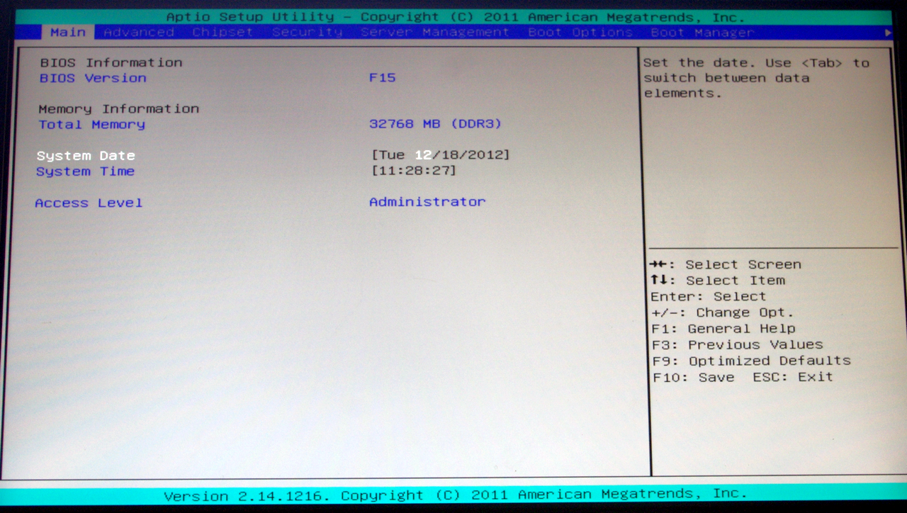
The front screen of the BIOS is basic at best, telling us the BIOS version, the total memory installed and the system date. Despite the market orientation for such a product, some indication as to what the motherboard is and the CPUs that are installed, at the bare minimum, would have been nice.
Apologies for the quality of the BIOS images – the BIOS has no ‘Print Screen to USB’ utility, and thus these images are taken with my DSLR in less-than-ideal lighting conditions.
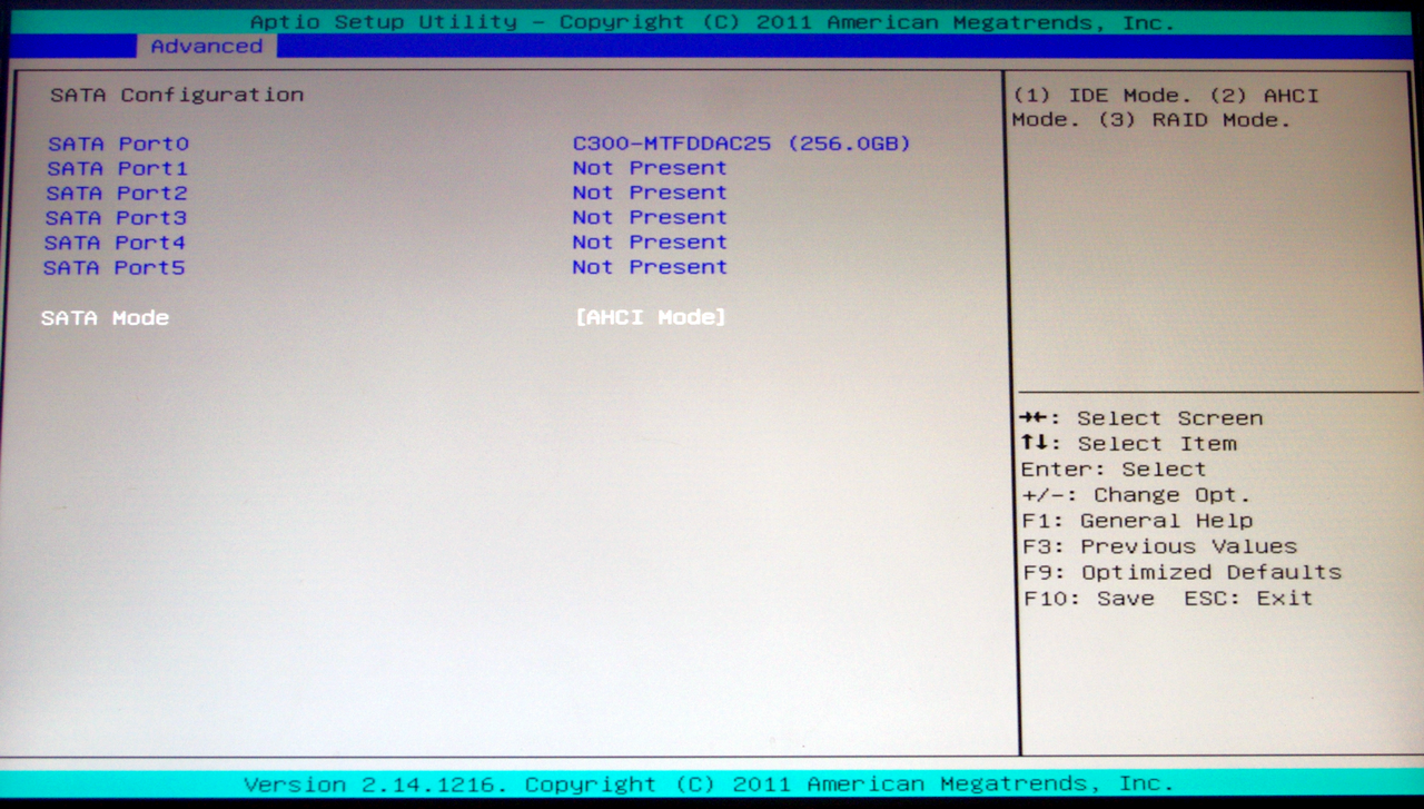
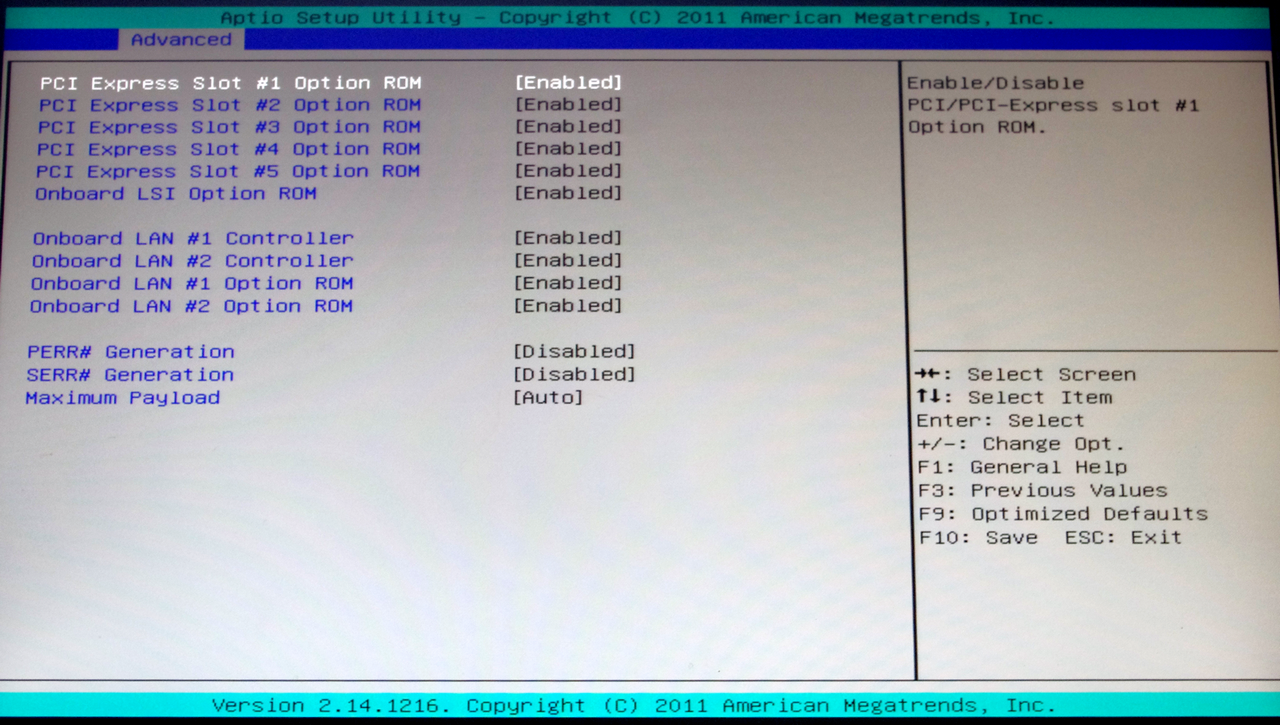
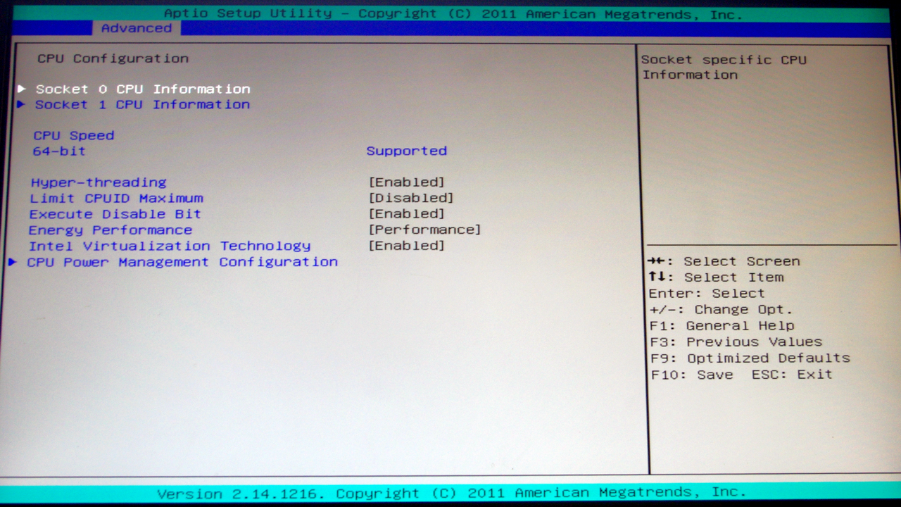
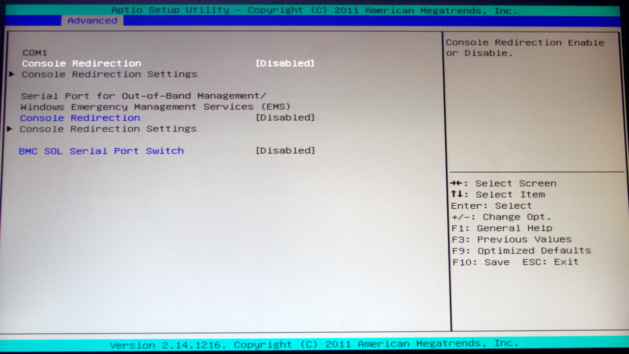
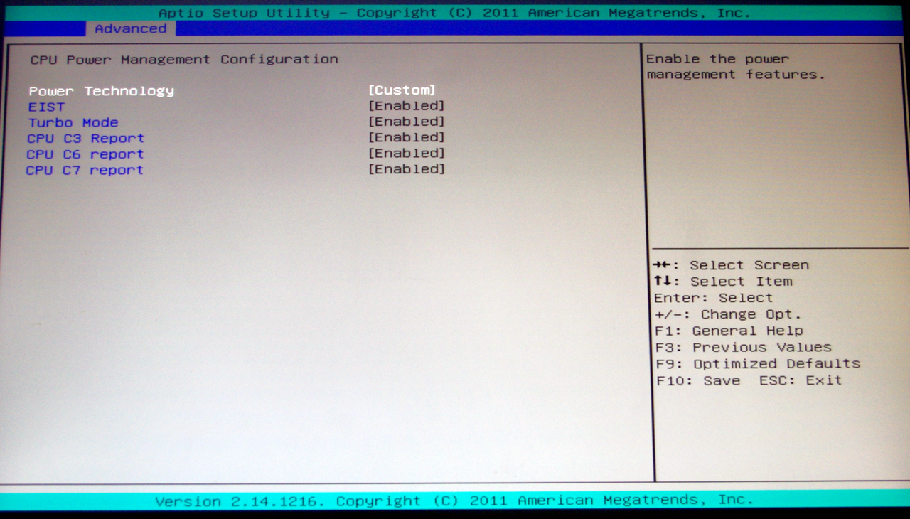
The Advanced menu tab has options relating to PCI Configuration, Trusted Computing (TPM), CPU identification and configuration (such as Hyperthreading and Power Management), error logging, SATA configuration, Super IO configuration and Serial Port options.
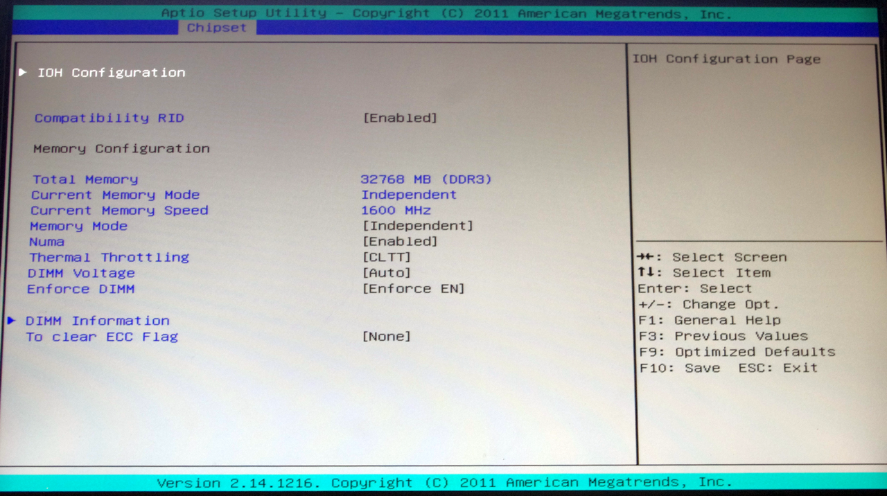
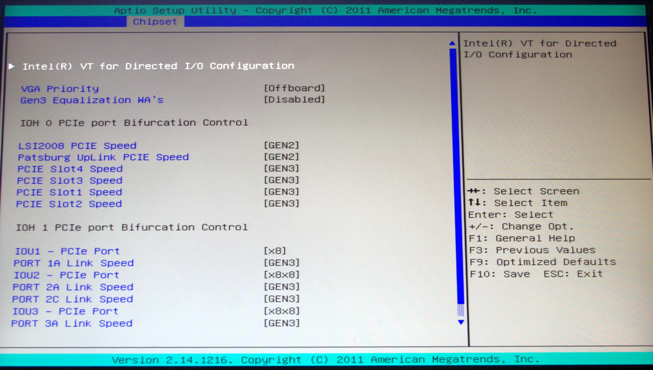
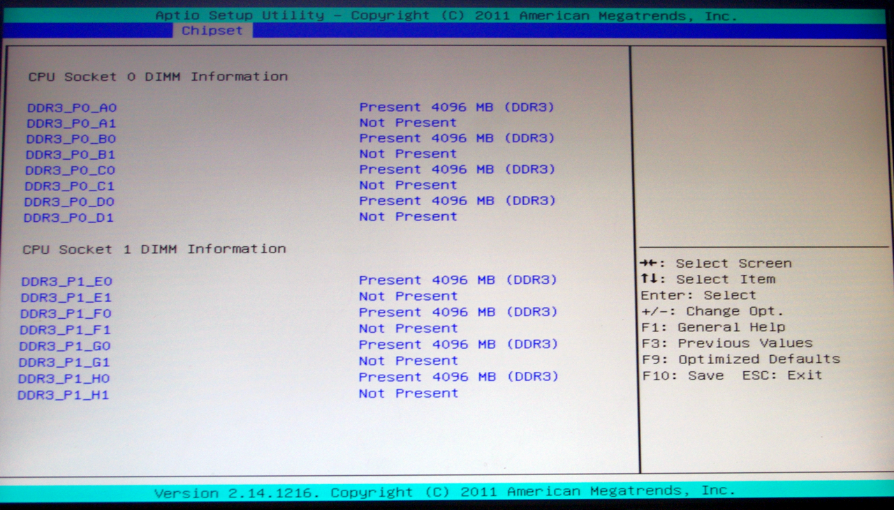
The Chipset tab option gives us access to North Bridge/South Bridge options, such as the memory controller, VT-d, PCIe lane counts and memory detection.
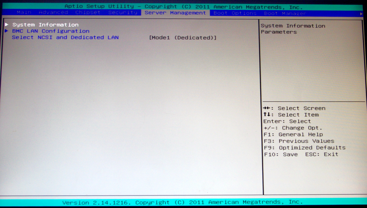
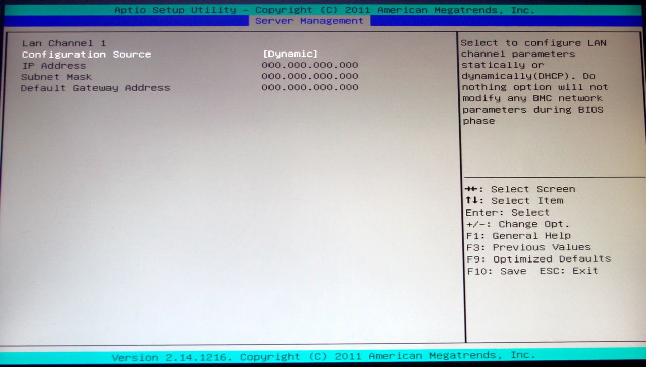
In order to access the server management features, after an ethernet cable has been plugged into the server management port, the IP for login details can be found in the server management tab:
Other options in the BIOS are for boot priority and boot override.


64 Comments
View All Comments
toyotabedzrock - Saturday, January 5, 2013 - link
There is a large number of very smart people on Google+. You really should come join us.JlHADJOE - Tuesday, January 8, 2013 - link
Of course there are lots of smart people on G+! You're all google employees right? =PActivate: AMD - Saturday, January 5, 2013 - link
As a fellow chemist, I must say that you have to be some kind of nut to want to do computational/physical chemistry. If you need me, I'll be at the bench!Good article too!
engrpiman - Saturday, January 5, 2013 - link
I didn't read the article in full but what I did read was top notch. I found your simulations and mathematics very interesting. I took a Physics class which was focused in writing code to run mathematical simulations . Using the given java lib. I wrote my own code to calculate PI. When I returned from the gym the program had calculated 3.1 . I then re-wrote the program from scratch and ditched the built in libs. and reran. I had 20 decimals in 30 sec it was an epic improvement.All in all I think your article could be very useful to me.
Thanks for writing.
SodaAnt - Saturday, January 5, 2013 - link
THIS is why I read Anandtech. I'll admit that I wasn't quite in the mood to read all the equations (I'll have to do that later), but really, these kind of reviews make my day.Cardio - Saturday, January 5, 2013 - link
Wonderful review...as always. ThanksHakon - Saturday, January 5, 2013 - link
Hi Ian. Thanks for the nice article. I have one suggestion regarding the explicit finite difference code:You could try to reorder the loops such that the memory access is more cache friendly. Right now 'pos' is incremented by NX (or even NX*NY in 3D) which will generate a lot cache misses for large grids. If you switch the x and the y loop (in the 2D case) this can be avoided.
IanCutress - Saturday, January 5, 2013 - link
Either way I order the loops, each point has to read one up, one down, one left and one right. My current code tries to keep three as consecutive reads and jump once, keeping the old jump in local memory. If I adjusted the loops, I could keep the one dimension in local memory, but I'd have to jump outside twice (both likely cache misses) to get the other data. I couldn't cache those two values as I never use them again in the loop iteration.When I did this code on the GPU, one method was to load an XY block into memory and iterate in the Z-dimension, meaning that each thread per loop iteration only loaded one element, with a few of them loading another for the halo, but all cache aligned.
I hope that makes sense :)
Ian
Hakon - Saturday, January 5, 2013 - link
Yes, but when you access the array 'cA' at 'pos' the CPU will fetch the entire cache line (64 byte in case of your machine, i.e. 16 floats) of the corresponding memory address into the CPU cache. That means that subsequent accesses to say 'pos + 1', 'pos + 2' and so on will be served by the cache. Accessing an array in such a sequential manner is therefore fast.However, when you access an array in a nasty way, e.g. 'NX + x' -> '2*NX + x', -> '3*NX + x', then each such access implies a trip to main memory if NX happens to be large.
That you need to move up / down and sideways in memory does not matter. When you write down the accesses of the code with the reordered loops you will notice that they just access three "lines" in memory in a cache friendly way.
Not reusing the old values of the last iteration should not affect performance in a measurable way. Even if the compiler fails to see this optimization, the accesses will be served by the L1 cache.
Btw, did you allocate the array having NUMA in mind, i.e. did you initialize your memory in an OpenMP loop with the same access pattern as used in the algorithms? I am a bit surprised by the bad performance of your dual Xeon system.
IanCutress - Saturday, January 5, 2013 - link
Memory was allocated via the new command as it is 1D. When using a 2D array the program was much slower. I was unaware you could allocate memory in an OpenMP way, which thinking about it could make the 2D array quicker. I also tried writing the code using the PPL and lambdas, but that was also slower than a simple OpenMP loop.I'm coming at these algorithms from the point of view of a non-CompSci interested in hardware, and the others in the research group were chemists content to write single threaded code on multi-core machines. Transferring the OpenMP variations of that code from a 1P to a 2P, as the results show, give variable results depending on the algorithm.
There are always ways to improve the efficiency of the code (and many ways to make it unreadable), but for a large part moving to the 2P system all depends on how your code performs. Please understand that my examples being within my limits of knowledge and representative of the research I did :) I know that SSE2/SSE4/AVX would probably help, but I have never looked into those. More often than not, these environments are all about research throughput, so rather than spend a few week to improve efficiency by 10% (or less), they'd rather spend that money getting a faster system which theoretically increases the same code throughput 100%.
I'll have a look at switching the loops if I write an article similar to this in the future :)
Ian