The Xeon Phi at work at TACC
by Johan De Gelas on November 14, 2012 1:44 PM EST- Posted in
- Cloud Computing
- CPUs
- IT Computing
- Intel
- Larrabee
- Xeon
- Xeon Phi
The Xeon Phi card comes on a PCIe card, much like a GPU. Given the architecture's origins as a GPU, the form factor should't come as a surprise. Like modern HPC GPUs however, the Xeon Phi card has no display output - its role is strictly for compute.
The Xeon Phi acts as a multi-core system on chip running its own operating system, a modified Linux kernel. Each Xeon Phi card has its own IP address however, the Xeon Phi can not operate on its own. A "normal" Xeon will be be the host CPU, the Xeon Phi card is a coprocessor, similar to the way your CPU and GPU work together.
Below you can see the SKUs that Intel will offer.
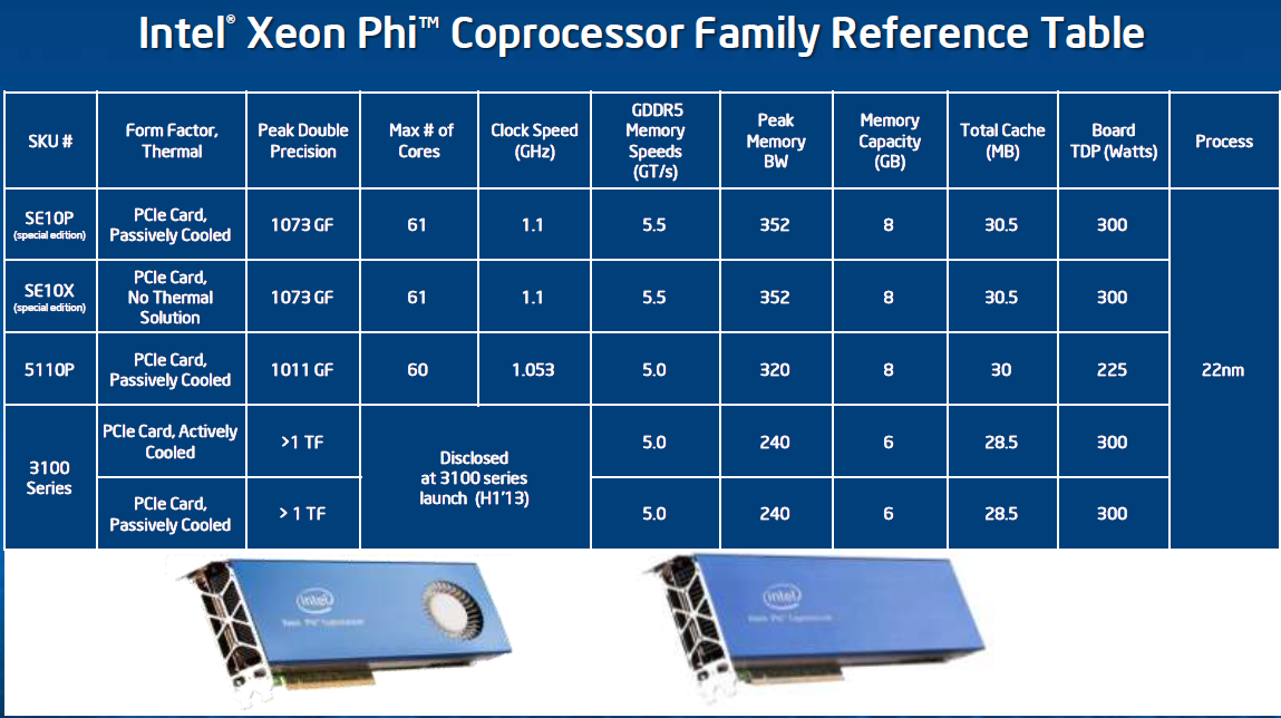
The Xeon Phi inside the Stampede are special edition Xeon Phis.These special editions get 61 cores and run at a slightly higher clockspeed (1.1 GHz).
The commercially avialable 5110P has one core and 50 MHz less than the special edition Phi but comes with 8 GB of ECC memory. The P-suffix indicates that it's passively cooled, relying on the host server for airflow. The 5110P is not cheap at $2699, but it's still more affordable than NVIDIA's Tesla K20 ($3199). The Xeon Phi 5100 series is really intended for more memory bandwidth bound applications thanks to the use of 5GHz GDDR5 and a fully populated 512-bit memory interface.
For compute bound applications however, Intel will offer the Xeon Phi 3100 series in the first half of next year for less than $2000. The Xeon Phi 3100 will come with 6GB of GDDR5 (5GHz data rate) and only a 384-bit memory interface. Core clock should be higher, delivering over 1TFLOP of DP FP performance.
The Xeon Phi cards use a 7GHz PCIe 2.0 interface, as Intel found moving to PCIe 3.0 resulted in slightly higher overhead.


46 Comments
View All Comments
creed3020 - Friday, November 16, 2012 - link
There are only 4 per row in the chassis because these units in Stampede feature the Xeon Phi card which requires a bigger sled. The author got the potential specs messed up with the way they are actually configured for this supercomputer.GullLars - Thursday, November 15, 2012 - link
So, it seems these are great at general purpose supercomputing.How do they stack up against the latest FPGAs if they are set up carefully by the people who will be running a specialized problem on them?
And would these be able to work effectively with offloading of some key functions that would be able to work 20-100x faster (or power efficient) on a carefully set up FPGA?
Some people in the comments mentioned hetrogenous computing. A step on the way is modular accelerated code. I'm interrested to see if we get more specialized hardware for acceleration in the comming years, not just graphics (with transcoding) and encryption/decryption like is common in CPUs now. Or if we get an FPGA component (integrated or PCIe) that can be reserved and set up by programs to realize huge speedups or power savings.
Jameshobbs - Monday, November 19, 2012 - link
Why have there not been a lot of reports regarding the PCI express. This was the first source that I was able to find that even mentions the speed of the PCI e bus for the Xeon Phi.One of the most challenging things for programming on accelerators is handling the PCI express and trying to balance data transfer with computational complexity. Everyone, NVIDIA, Intel, AMD seem to be doing a lot of arm waving regarding this issue, and there are many GPU papers that tend to omit the transfer times in their results. To me I find this dishonest and cheating.
One thing that continues to shock me as well is that people keep complaining about how difficult it is to debug a GPU program and then they reference old out of date references such as http://lenam701.blogspot.be/2012/02/nvidia-cuda-my... which was mentioned above. The things that the author of that blog post complained about have been resolved in the latest versions of CUDA (from 4.2 onward... maybe even in 4.0).
Programmers can now use printf and it is possible to hook a debugger into a GPU application to do more in depth debugging. The main thing that bothers me about GPU programming is you must check to make sure a program has successfully completed or not. Other than that I find it relatively easy to debug a GPU application.
MySchizoBuddy - Wednesday, November 21, 2012 - link
Next version of AMD APU will allow both the GPU and CPU access to the same memory locations.sheepdestroyer - Wednesday, December 5, 2012 - link
i would really like to see a benchmark of this cpu on LLVMpipehttp://www.mesa3d.org/llvmpipe.html
The original Larabee would have had a DirectX translation layer and this project could be seen as an OpenGL version of it.
Just loading a distro with Gnome 3 running on LLVMpipe or benchmarking some ioq3 and iodoom3 games would be VERY interesting.
tuklap - Sunday, March 3, 2013 - link
Can this accelerate my normal PC applications like Rendering in AutoCAD/Revit, Media Conversion, STAAD, ETABS and etc computations???or do i Have to create my own applications?