Google Nexus 4 Review - Google's new Flagship
by Brian Klug on November 13, 2012 8:45 AM EST- Posted in
- Smartphones
- LG
- Android
- Mobile
- APQ8064
- Nexus 4
- Android 4.2
- MDM9215
I usually take apart smartphones I’m sampled just because I like knowing what’s inside, even if I already know the majority of component choices through other purely software means. In the case of the Nexus 4 this was also motivated by my desire to find out whether it would be possible to replace the battery easily and also to get a look at some of the RF components for cellular.


Taking apart the Nexus 4 is surprisingly simple, so much so that I’ve taken my Nexus 4 review unit apart fully, twice. There are two Torx T–4 screws at the bottom which come out, after which the back cage pulls off after you use a plastic separator tool to get past some clips holding it on. If you’re interested in replacing the battery you can pretty much stop here, there are two screws holding the battery connector onto the mainboard, and the battery is held in place with a square outline of double sided tape. The back side of the case has many gold pads for antennas, NFC, and the inductive charging coils.

Further disassembly involves removing the plastic covering the PCB, then a few screws and the mainboard lifts out. Construction here is very standard fare for smartphones lately, with an L shaped mainboard and battery sitting in the cavity next to it.
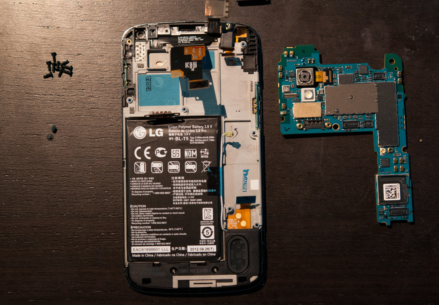
After you get the PCB out things are very easy to identify. I popped the EMI cans off wherever possible as well.
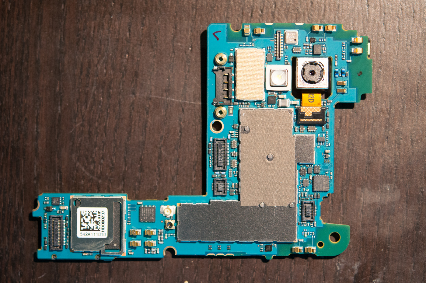
First off on the backside we can see the DRAM PoP atop APQ8064, which in this case is Samsung 2x32-bit LPDDR2–1066, 2GB courtesy of 4 x 512MB die at 1.2V. Below that is the Qualcomm MDM9215 baseband, to the left we can see the baseband PMIC (PM8821), and to the left of that the PMIC for APQ8064, PM8921.
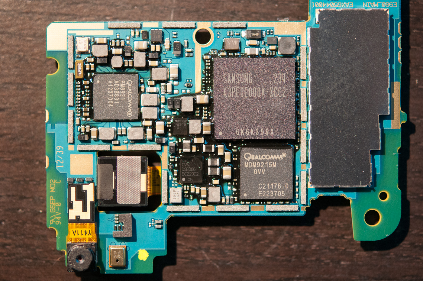
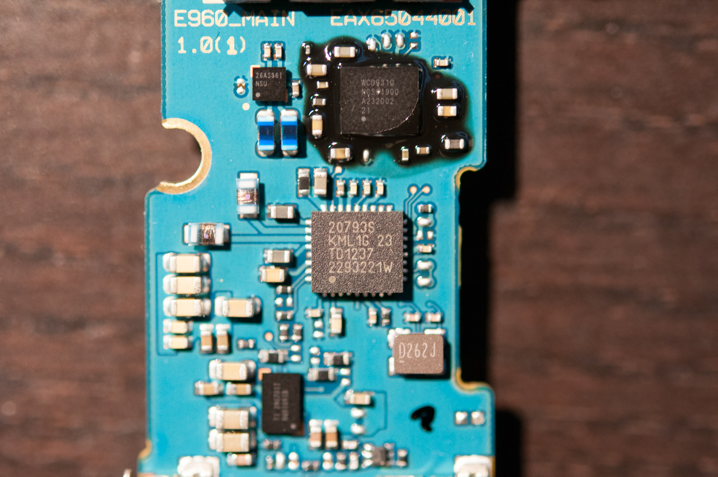
On the long underside of the mainboard we can see the TI BQ51051b wireless power Li-Ion charger receiver I mentioned earlier, and above it Qualcomm’s WCD9310 Audio codec in a sea of epoxy. Inbetween those two is a BCM20793 NFC controller instead of the ubiquitous NXP PN544 part.
My main goal when taking apart the Nexus 4 was nailing down what power amplifiers and RF architecture the phone had, and under the EMI cans on this side are a few relevant parts.
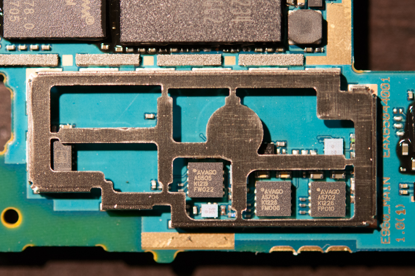
There are three Avago power amplifiers, and an RFMD switch at left. We can see Avago A5505 (Band 5 - UMTS), A5704 (Band 4 - LTE/UMTS), A5702 (Band 2 - LTE/UMTS), and at far left an RFMD 1156 single pole 5 throw switch hiding under a lip of the EMI can.
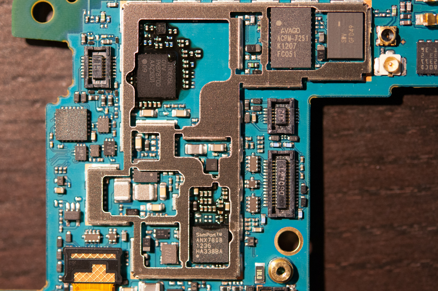
Flipping the PCB over and removing the other large EMI can reveals more parts of the puzzle. I can identify an Avago ACPM–7251 (Band 1, 5, Quad band GSM/EGE) power amplifier, and another package near it marked “GFD49” which is probably another switch just next to the antenna feed for the bottom transmit antenna.

Nexus 4 also has the latest and greatest Qualcomm transceiver onboard, WTR1605L, which we’re going to talk at length about in another piece. It’s actually somewhat surprising to see the latest and greatest here considering the Nexus 4 doesn’t include LTE support, even though it does have the hardware for it on bands 4, 2, and 1 in theory.
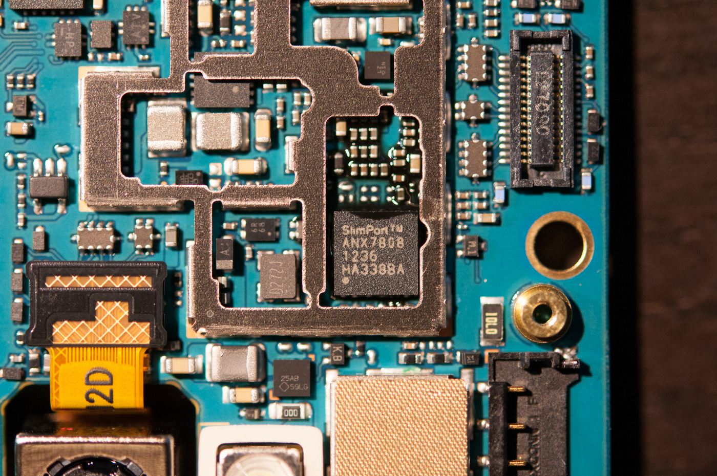
Also under this can is the SlimPort ANX7808 which enables HDMI, VGA, DVI, or DisplayPort out on the Nexus 4 instead of the USB-MHL that we’ve been seeing getting adoption pretty rapidly. This is actually an interesting choice for the Nexus 4 considering again the relative ubiquity of MHL. I don’t have any SlimPort cables or dongles so I can’t test it first hand, but there’s the transmit package on the PCB that enables it.

I can also identify an InvenSense MPU–6050 six axis gyro and accelerometer at the very top of the PCB.

I couldn’t get the can off of what appears to be the eMMC (the only remaining large package), we’ll have to see if anyone else wants to do some destructive digging to get that one. Finally the Nexus 4 also has a linear actuator vibrator which you can see in the FCC teardown photos.


188 Comments
View All Comments
dishayu - Wednesday, November 14, 2012 - link
Meh, that is how they statistically show you that thermal throttling is affecting the performance. Your accusation would have help good if they had only published the freezer benchmarks. But they published both because they wanted to showcase that the phone thermally throttles itself (i.e. a negative point about the phone)... How exactly is that partial?kgh00007 - Monday, November 19, 2012 - link
I think it is particularly significant that this phone was selected to be the first phone that was actually put in a freezer and the results published, why not the iPhone or some other phone that was known to be trottling?Seriously, think about it.
There is a big difference between stating that a phone throttles and the theoretical performance is X and actually putting a phone in the freezer and publishing the resulting benchmarks.
I am entitled to my opinion, and my opinion here is that somebody is working for the man, the wrong man.
kgh00007 - Monday, November 19, 2012 - link
There is quite a big difference between stating that a phone is throttling and the theoretical performance should be X, and putting a phone in the freezer and publishing the resulting benchmarks.The choice of phone to be the first to recieve this treatment is suspicious to me.
My opinion, which I am entitled to, is that somebody is working for the man, the wrong man.
This is evident to me, think about it yourself.
thesavvymage - Wednesday, November 14, 2012 - link
they basically said "the phone IS being thermally throttled. here's what would happen if it wasnt..."nowhere does it ever say that the freezer tests would ever be indicative of a real world test. they are just showing for information
kgh00007 - Monday, November 19, 2012 - link
People are aready taklking in the comments about how this phone has to be put in the freezer in order to gain maximum performance from it.People are not saying the same about the iPhone, that is the significance.
As I said something fishy going on here and I don't like it.
In fact this is the first time Anandtech has dissapointed me with a review, but it is a rather large dissapointment.
galtma - Wednesday, November 14, 2012 - link
Is it feasible to replace the RAM in the N4 to upgrade it to 32gb? Where in the internals would you dig?noblemo - Wednesday, November 14, 2012 - link
I think you are referring to the NAND Flash, but in either case the NAND and RAM are soldered to the mainboard. Brian made the following comment in the section, "Inside the Nexus 4" (page 7 of the review) regarding the NAND:"I couldn’t get the can off of what appears to be the eMMC (the only remaining large package), we’ll have to see if anyone else wants to do some destructive digging to get that one."
He is referring to the device under the EMI shield (with a QR code label) in the lower left corner of this image:
http://images.anandtech.com/galleries/2435/Nexus-4...
praveen44 - Wednesday, November 14, 2012 - link
Excellent review.spiritrajat - Wednesday, November 14, 2012 - link
most exhaustive review..being an electronics engg myself i realy enjoyed going through the reveiw...job very well donenoblemo - Wednesday, November 14, 2012 - link
Q: Hey, Nexus 4, why so blue?A: Because no one at Google is responsible for display calibration.
It's unfortunate that color accuracy does not get more attention from manufacturers.
Was throttling observed and was there a noticeable impact during daily usage? Any thoughts on whether it would be an issue in climates with ambient temperatures greater than 30C?