Intel's Haswell Architecture Analyzed: Building a New PC and a New Intel
by Anand Lal Shimpi on October 5, 2012 2:45 AM ESTWhen I first started writing about x86 CPUs Intel was on the verge of entering the enterprise space with its processors. At the time, Xeon was a new brand, unproven in the market. But it highlighted a key change in Intel's strategy for dominance: leverage consumer microprocessor sales to help support your fabs while making huge margins on lower volume, enterprise parts. In other words, get your volume from the mainstream but make your money in the enterprise. Intel managed to double dip and make money on both ends, it just made substantially more in servers.
Today Intel's magic formula is being threatened. Within 8 years many expect all mainstream computing to move to smartphones, or whatever other ultra portable form factor computing device we're carrying around at that point. To put it in perspective, you'll be able to get something faster than an Ivy Bridge Ultrabook or MacBook Air, in something the size of your smartphone, in fewer than 8 years. The problem from Intel's perspective is that it has no foothold in the smartphone market. Although Medfield is finally shipping, the vast majority of smartphones sold feature ARM based SoCs. If all mainstream client computing moves to smartphones, and Intel doesn't take a dominant portion of the smartphone market, it will be left in the difficult position of having to support fabs that no longer run at the same capacity levels they once did. Without the volume it would become difficult to continue to support the fab business. And without the mainstream volume driving the fabs it would be difficult to continue to support the enterprise business. Intel wouldn't go away, but Wall Street wouldn't be happy. There's a good reason investors have been reaching out to any and everyone to try and get a handle on what is going to happen in the Intel v ARM race.
To make matters worse, there's trouble in paradise. When Apple dropped PowerPC for Intel's architectures back in 2005 I thought the move made tremendous sense. Intel needed a partner that was willing to push the envelope rather than remain content with the status quo. The results of that partnership have been tremendous for both parties. Apple moved aggressively into ultraportables with the MacBook Air, aided by Intel accelerating its small form factor chip packaging roadmap and delivering specially binned low leakage parts. On the flip side, Intel had a very important customer that pushed it to do much better in the graphics department. If you think the current crop of Intel processor graphics aren't enough, you should've seen what Intel originally planned to bring to market prior to receiving feedback from Apple and others. What once was the perfect relationship, is now on rocky ground.
The A6 SoC in Apple's iPhone 5 features the company's first internally designed CPU core. When one of your best customers is dabbling in building CPUs of its own, there's reason to worry. In fact, Apple already makes the bulk of its revenues from ARM based devices. In many ways Apple has been a leading indicator for where the rest of the PC industry is going (shipping SSDs by default, moving to ultra portables as mainstream computers, etc...). There's even more reason to worry if the post-Steve Apple/Intel relationship has fallen on tough times. While I don't share Charlie's view of Apple dropping Intel as being a done deal, I know there's truth behind his words. Intel's Ultrabook push, the close partnership with Acer and working closely with other, non-Apple OEMs is all very deliberate. Intel is always afraid of customers getting too powerful and with Apple, the words too powerful don't even begin to describe it.
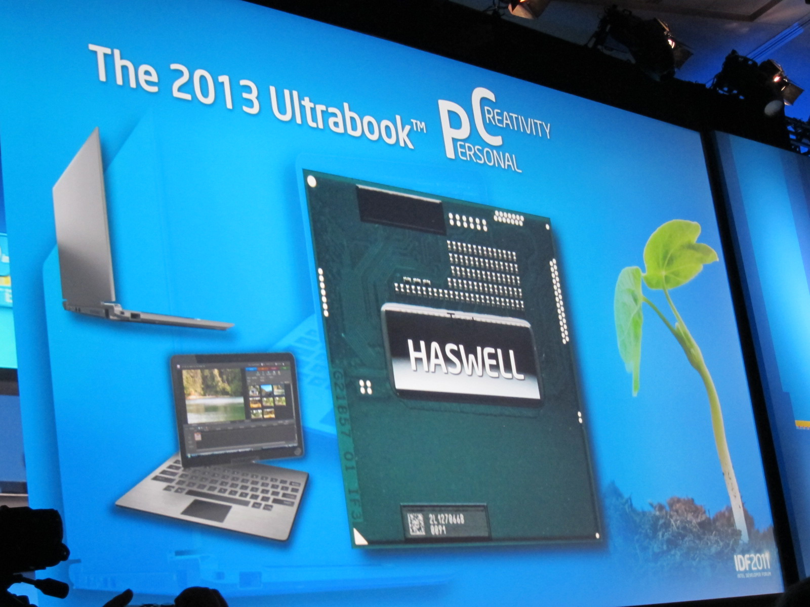
What does all of this have to do with Haswell? As I mentioned earlier, Intel has an ARM problem and Apple plays a major role in that ARM problem. Atom was originally developed not to deal with ARM but to usher in a new type of ultra mobile device. That obviously didn't happen. UMPCs failed, netbooks were a temporary distraction (albeit profitable for Intel) and a new generation of smartphones and tablets became the new face of mobile computing. While Atom will continue to play in the ultra mobile space, Haswell marks the beginning of something new. Rather than send its second string player into battle, Intel is starting to prep its star for ultra mobile work.
Haswell is so much more than just another new microprocessor architecture from Intel. For years Intel has enjoyed a wonderful position in the market. With its long term viability threatened, Haswell is the first step of a long term solution to the ARM problem. While Atom was the first "fast-enough" x86 micro-architecture from Intel, Haswell takes a different approach to the problem. Rather than working from the bottom up, Haswell is Intel's attempt to take its best micro-architecture and drive power as low as possible.


245 Comments
View All Comments
Da W - Friday, October 5, 2012 - link
AMD spend 1/10th of Intel in R&D. There are things they just cant do, i suspect pursuing higher x86 single trend performance is one of them.StevoLincolnite - Saturday, October 6, 2012 - link
However, allot of the R&D Intel spends is on lithography type technologies, AMD doesn't have to spend Billions on such things anymore.Besides, a simple way for AMD to beat Intel when Intel is a node ahead is to throw more transistors at the problem which they have succeeded very well at doing in the past.
Mind you, that comes at the cost of power and die size, however with stuff like clock mesh it can negate some of that.
Kevin G - Friday, October 5, 2012 - link
Being four steps behind ARM isn't necessarily a bad thing unless you're trying to leap frog them. AMD appears to be content with letting Intel spearhead the effort to get into the ultramobile market. With Intel two steps behind of ARM and they couldn't leap frog over ARM, there is little chance that AMD would be able to do the same. It isn't just knowing what battles to fight but also when to fight them.abufrejoval - Friday, October 5, 2012 - link
It was only when I was reading Jana Rutkowska's notes on the current UI limitations within Qubes, that I finally understood (I believe!) the message which AMD has been pushing for quite a few years now: GPU compute will truly be an integral part of their future APUs in one or two generations, becoming almost an augmented instruction set instead of just a SoC.Currently all Qubes "user" applications, that is everything except the Dom0, can't use the GPU to render their graphics: It's basically software rendering into an off-screen composition buffer and then GPU assisted composition of these software buffers onto the visible screen (this time with all the wobble and transition effects we've all come to expect and love ;-)
That's because although the GPU is on the same die even on the newest Trinity class APUs, it's still logically very separate, sharing only some stuff but bypassing, I believe, the ordinary page tables (not the IOMMU ones) and the snooping logic for caches. So even if GPU and CPU sit on the same die and use the same phyiscal DRAM bus, doing GPU compute implies using a dedicated part of that RAM in a way, which doesn't mesh seamlessly with CPU compute.
But the roadmap seems to imply, that this limitation will go away, which would allow e.g. Qubes to use GPU assisted rendering anywhere in user space memory and thus also into a per DomU virtual framebuffer composed of quite ordinary paged virtual memory, which could then be assembled by the Dom0 for the visible screen or for video encoding and streaming to a remote display device e.g. for cloud gaming.
This easy feeding of GPU "results" into another software layer is currently either impossible or requires major fiddling with device drivers so it's limited to the GPU vendors and bilateral deals such as nVidia and Splashtop. Once the GPU becomes more of an augmented instruction set, allowing OpenCL or even hardware primitives on ordinary user space paged virtual memory, this becomes as natural as running virtual machines with hardware virtualization.
And at that point even the new 256bit FMA may look pretty lame compared to what hundreds of APU EUs could do. That to me explains rather well, why AMD isn't spending more transistors on a vastly improved CPU only x86 ISA: It truly belives it's a dead end for both personal and scientific workloads.
It's a very daring bet and I very much admire them for having the vision and the balls to tie the company's survival to it. Over the last 40 years Intel seems to have failed with most of its visions (80432, i860, Itanium), but excelled on evolving x86. AMD, however, seems better on vision and noticably 2nd rate on execution.
APUs are potentially quite dangerous both to nVidia and to Intel, because both can't easily duplicate them: The AMD/Intel cross licensing deal IMHO won't cover the GPU portion. Unless nVidia and Intel join, which would only happen if either of the two is in truly dire straights.
But quite a few things need to fall in place over the next couple of years and AMD needs to survive them for that potential to develop. And it looks like all ther other players aren't standing still.
Events like Apple potentially using Samsung augmented cash billions to turn TMSC into a private provider of 1x nm ARM SoCs are sending shock waves into the market, which may force "strange" alliances.
These days when even trival things like "swipe to unlock" can be patented and used to bloodlet competitors I'm surprised to see IBM and Intel use things like transactional memory, which saw silocon first with Sun's Rock, I believe, or Intel turning to eDRAM for caches and frame buffers, which IBM's been implementing first on the p-Series.
That leads me to an open question on the commercial workloads, which is almost the only domain, where I have difficulties seeing the immediate benefit of APUs, at least after Oracle's grab on Java and their expressed intent to make commercial workloads a SPARC exclusive (please see Larry's opening remarks on Openworld 2012): How can AMD make APUs the better Java and database engines? How can they make search, big data, map reduced or JavaScript run better on APUs?
I can only guess that having managed CPU+GPU AMD would be in a better position to add xPU for all of the above.
ltcommanderdata - Friday, October 5, 2012 - link
A great, detailed description of Haswell's architecture. I do have some questions though.You mentioned that Intel will be including up to 1 redundant EU in the GPU array. Does that mean only GT3 will have the 1 redundant EU (41 total, 40 usable) with GT2 having no redundancy? Or is it 1 redundant EU per sub-slice, so GT2 will have 1 and GT3 will have 2?
Will the embedded DRAM be implemented PoP like in SoC? When you say we'll see a version of Haswell with embedded DRAM do will all GT3 have embedded DRAM or will only some GT3 have embedded DRAM (kind of a GT4)?
Given the long timescales of CPU design, there would be overlap between the Haifa team working on Sandy Bridge/Ivy Bridge (particularly Ivy Bridge) and the Hillsboro team working on Haswell. I was wondering if you knew how much opportunity there is for learning between consecutive designs in terms of magnitude of changes possible and timescales before things are pretty much fixed? I'm in no position to judge, but I was also wondering based on your knowledge of the architectures and/or interactions with members of the design teams if you sense any distinct difference in design philosophies between the Haifa and Hillsboro teams. Afterall, the Haifa team's background was in power-efficient, mobile-oriented designs whereas Hillsboro was high-performance, desktop/server oriented. You mentioned in the article that Haswell goes back to Nehalem's 3 clock domains due to lessons learned from Sandy Bridge/Ivy Bridge. While I don't doubt that's the primary reason, I wonder if design philosophy played a role too since Nehalem and Haswell are both Hillsboro designs and maybe they like 3 clock domains.
Anand Lal Shimpi - Friday, October 5, 2012 - link
Unfortunately that's all the info I have on redundancy in the GPU array. I think we'll have to wait until we're closer to launch to know more. The same goes for the nature of the on-package memory.I wondered the same thing about the correlation between design teams and decisions in Nehalem/Haswell, I refrained from speculating on it in the article because I didn't necessarily see any reason to doing so, but I definitely noticed the same correlation. It could just be a coincidence though. Nothing else beyond the L3 cache frequency really stood out to me as being an obvious common thread between Nehalem and Haswell though.
Take care,
Anand
ltcommanderdata - Friday, October 5, 2012 - link
Thanks again for your insights.tipoo - Friday, October 5, 2012 - link
Speaking of the EUs, is the GT3 part twice as fast as the HD4000 with or without the eDRAM cache? The article seems to imply with, but then what is the performance without it if they've doubled the EUs? Doesn't it seem more likely they doubled performance without the cache, and the cache doubles it beyond that?telephone - Friday, October 5, 2012 - link
Anand, thanks for the insights. We all enjoyed it very much and look forward to getting the real thing into your labs.To clarify some questions:
As for the design team philosophy, the Hillsboro design team continually tries to outdo the Haifa design team and vice versa. Both teams have access to the other teams' design collateral, as we co-own the tick-tock model.
Next, the reasons for the "3" clock domains are too complicated (and confidential) to go into. Since designing for "2" clock domains is much simpler, the reason is not that we enjoy pain and misery. Suffice to say, that you are missing a very big piece of the puzzle and accurate conclusions as to why this was done cannot be drawn from the information you have. And the number of clock domains is in quotes because those are not accurate anyhow.
Sincerely,
Someone from the Hillsboro Design Team
Stahn Aileron - Friday, October 5, 2012 - link
I'm curious as to whether Intel has enough interest to drive the Atom design low enough to hit ARM power level (like Medfield) and integrate an Atom core into a Core CPU design. nVidia introduced a heterogeneous CPU in their Tegra 3 SoC. (Two different ARM core types in the CPU block). From all the stuff I've seen about Intel over the past half decade, I'm pretty sure they have the resources to pull that off. They have top-notch designers and engineers with the basic tech and designs need to start R&D on that, I think.On the other hand, if they really are trying to force a Core design in Atom territory... Well, hell ya ^_~ Still, I can't really see Core hitting the sub-1W power levels they've been able to do with Atom (Medfield). I figure using an Atom core for basic S0ix functions would be a little more power efficient than using a Core design, but I'm no silicon engineer. Intel would know about that far better than me.