Intel's Haswell Architecture Analyzed: Building a New PC and a New Intel
by Anand Lal Shimpi on October 5, 2012 2:45 AM ESTDecoupled L3 Cache
With Nehalem Intel introduced an on-die L3 cache behind a smaller, low latency private L2 cache. At the time, Intel maintained two separate clock domains for the CPU (core + uncore) and a third for what was, at the time, an off-die integrated graphics core. The core clock referred to the CPU cores, while the uncore clock controlled the speed of the L3 cache. Intel believed that its L3 cache wasn't incredibly latency sensitive and could run at a lower frequency and burn less power. Core CPU performance typically mattered more to most workloads than L3 cache performance, so Intel was ok with the tradeoff.
In Sandy Bridge, Intel revised its beliefs and moved to a single clock domain for the core and uncore, while keeping a separate clock for the now on-die processor graphics core. Intel now felt that race to sleep was a better philosophy for dealing with the L3 cache and it would rather keep things simple by running everything at the same frequency. Obviously there are performance benefits, but there was one major downside: with the CPU cores and L3 cache running in lockstep, there was concern over what would happen if the GPU ever needed to access the L3 cache while the CPU (and thus L3 cache) was in a low frequency state. The options were either to force the CPU and L3 cache into a higher frequency state together, or to keep the L3 cache at a low frequency even when it was in demand to prevent waking up the CPU cores. Ivy Bridge saw the addition of a small graphics L3 cache to mitigate this situation, but ultimately giving the on-die GPU independent access to the big, primary L3 cache without worrying about power concerns was a big issue for the design team.
When it came time to define Haswell, the engineers once again went to Nehalem's three clock domains. Ronak (Nehalem & Haswell architect, insanely smart guy) tells me that the switching between designs is simply a product of the team learning more about the architecture and understanding the best balance. I think it tells me that these guys are still human and don't always have the right answer for the long term without some trial and error.
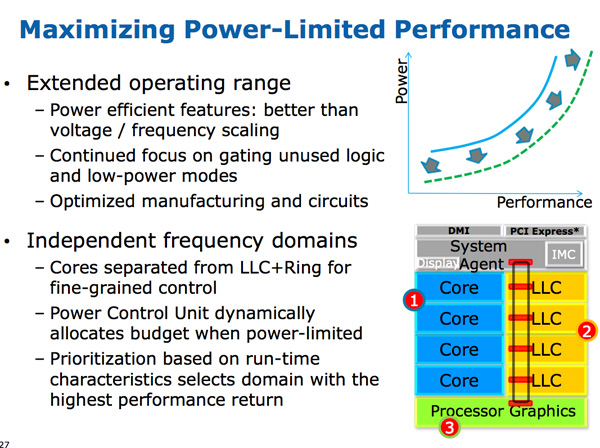
The three clock domains in Haswell are roughly the same as what they were in Nehalem, they just all happen to be on the same die. The CPU cores all run at the same frequency, the on-die GPU runs at a separate frequency and now the L3 + ring bus are in their own independent frequency domain.
Now that CPU requests to L3 cache have to cross a frequency boundary there will be a latency impact to L3 cache accesses. Sandy Bridge had an amazingly fast L3 cache, Haswell's L3 accesses will be slower.
The benefit is obviously power. If the GPU needs to fire up the ring bus to give/get data, it no longer has to drive up the CPU core frequency as well. Furthermore, Haswell's power control unit can dynamically allocate budget between all areas of the chip when power limited.
Although L3 latency is up in Haswell, there's more access bandwidth offered to each slice of the L3 cache. There are now dedicated pipes for data and non-data accesses to the last level cache.
Haswell's memory controller is also improved, with better write throughput to DRAM. Intel has been quietly telling the memory makers to push for even higher DDR3 frequencies in anticipation of Haswell.


245 Comments
View All Comments
defiler99 - Tuesday, October 16, 2012 - link
One of the best articles on Anandtech in some time. This is great original tech industry reporting.Gc - Saturday, January 12, 2013 - link
Congratulations, an intel cpu engineer wrote around 27 Dec 2012:"... Anandtech's latest Haswell preview is also excellent; missing some key puzzle pieces to complete the picture and answer some open questions or correct some details but otherwise great. ..."
http://www.reddit.com/r/IAmA/comments/15iaet/iama_...
xaml - Thursday, May 23, 2013 - link
This was first posted here a few handfuls of pages back as a comment by user "telephone". ^^yhselp - Friday, March 29, 2013 - link
A few questions.Is there going to be a replacement (37W) for the current IVB 35W quad-core part? Quite a few designs are now dependable on this, lower power quad-core option - Sony S-series and Razer Blade, to name a few.
When can we expect all mobile CPUs (except maybe for the extreme series) to fall into the 10W-20W range? In three years' time and 10nm?
The decision to not include GT3 with desktop parts is very disappointing. A 35/45W low-voltage part with GT3 would make for an excellent HTPC build, among other things. Is there a chance Intel change their mind and start shipping GT3 desktop parts at some point?
JVimes - Tuesday, August 19, 2014 - link
Does EU stand for Execution Unit? That was surprisingly hard to google for.