Intel's Haswell Architecture Analyzed: Building a New PC and a New Intel
by Anand Lal Shimpi on October 5, 2012 2:45 AM ESTHaswell's GPU
Although Intel provided a good amount of detail on the CPU enhancements to Haswell, the graphics discussion at IDF was fairly limited. That being said, there's still some to talk about here.
Haswell builds on the same fundamental GPU architecture we saw in Ivy Bridge. We won't see a dramatic redesign/re-plumbing of the graphics hardware until Broadwell in 2014 (that one is going to be a big one).
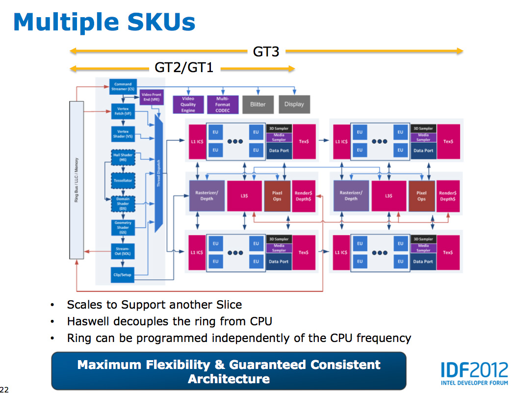
Haswell's GPU will be available in three physical configurations: GT1, GT2 and GT3. Although Intel mentioned that the Haswell GT3 config would have twice the shader count of Haswell GT2, it was careful not to disclose the total number of EUs in any of the versions. Based on the information we have at this point, GT3 should be a 40 EU configuration while GT2 should feature 20 EUs. Intel will also be including up to one redundant EU to deal with the case where there's a defect in an EU in the array. This isn't an uncommon practice, but it does indicate just how much of the die will be dedicated to graphics in Haswell. The larger of an area the GPU covers, the greater the likelihood that you'll see unrecoverable defects in the GPU. Redundancy at the EU level is one way of mitigating that problem.
Haswell's processor graphics extends API support to DirectX 11.1, OpenCL 1.2 and OpenGL 4.0.
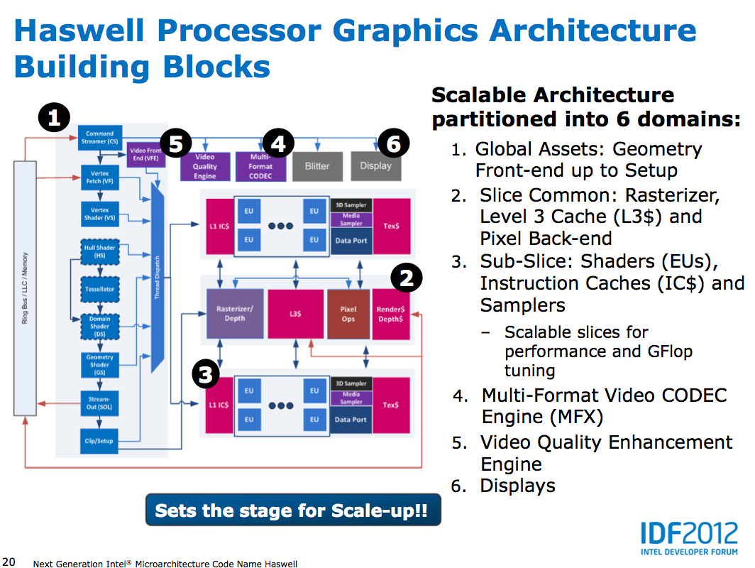
At the front of the graphics pipeline is a new resource streamer. The RS offloads some driver work that the CPU would normally handle and moves it to GPU hardware instead. Both AMD and NVIDIA have significant command processors so this doesn't appear to be an Intel advantage although the devil is in the (unshared) details. The point from Intel's perspective is that any amount of processing it can shift away from general purpose CPU hardware and onto the GPU can save power (CPU cores go to sleep while the RS/CS do their job).
Beyond the resource streamer, most of the fixed function graphics hardware sees a doubling of performance in Haswell.
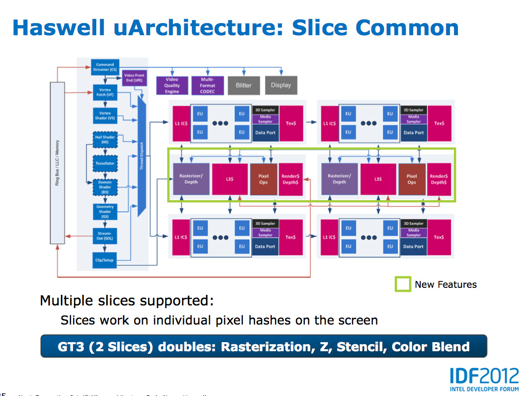
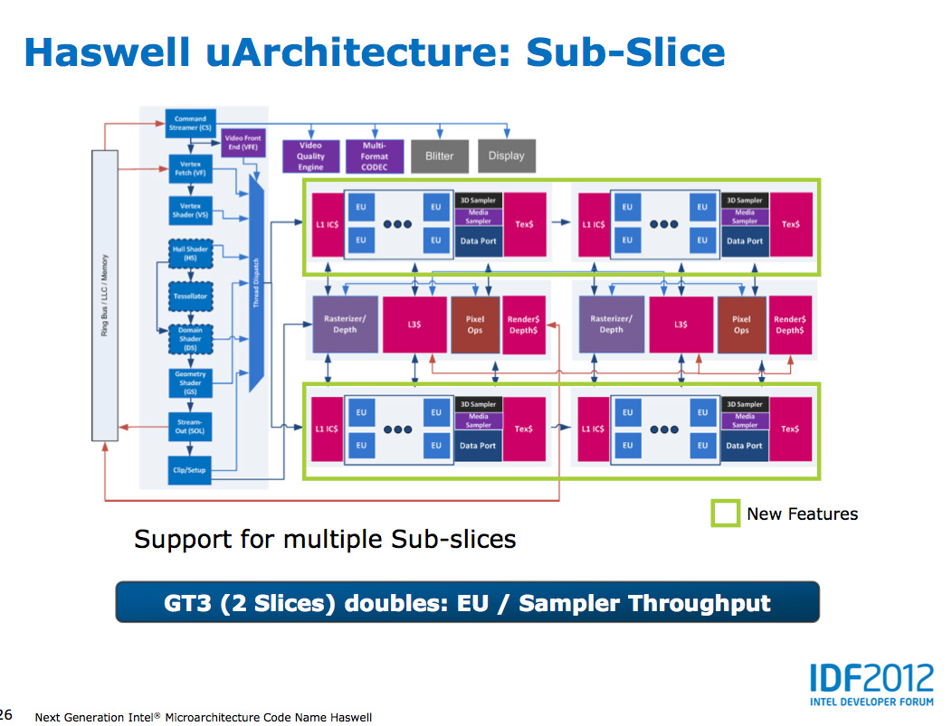
At the shader core level, Intel separates the GPU design into two sections: slice common and sub-slice. Slice common includes the rasterizer, pixel back end and GPU L3 cache. The sub-slice includes all of the EUs, instruction caches and EUs.
In Haswell GT1 and GT2 there's a single slice common, while GT3 sees a doubling of slice common. GT3 similarly has two sub-slices, although once again Intel isn't talking specifics about EU counts or clock speeds between GT1/2/3.
The final bit of detail Intel gave out about Haswell's GPU is the texture sampler sees up to a 4x improvement in throughput over Ivy Bridge in some modes.
Now to the things that Intel didn't let loose at IDF. Although originally an option for Ivy Bridge (but higher ups at Intel killed plans for it) was a GT3 part with some form of embedded DRAM. Rumor has it that Apple was the only customer who really demanded it at the time, and Intel wasn't willing to build a SKU just for Apple.
Haswell will do what Ivy Bridge didn't. You'll see a version of Haswell with up to 128MB of embedded DRAM, with a lot of bandwidth available between it and the core. Both the CPU and GPU will be able to access this embedded DRAM, although there are obvious implications for graphics.
Overall performance gains should be about 2x for GT3 (presumably with eDRAM) over HD 4000 in a high TDP part. In Ultrabooks those gains will be limited to around 30% max given the strict power limits.
As for why Intel isn't talking about embedded DRAM on Haswell, your guess is as good as mine. The likely release timeframe for Haswell is close to June 2013, there's still tons of time between now and then. It looks like Intel still has a desire to remain quiet on some fronts.


245 Comments
View All Comments
rundll - Friday, October 5, 2012 - link
Four cores and 95 W tdp.What is this?
meloz - Friday, October 5, 2012 - link
Yes this caught my eye and I would like an answer, too.Maybe it is one SKU with GT3 for desktop? Or maybe it is a 6 core part?
Or maybe.....it is the mother of all overclocking processors. Muhahahahah!
Kevin G - Friday, October 5, 2012 - link
I suspect that 95W is the rated socket limit. This is similar to how Intel advertises Ivy Bridge at 77 W on the desktop but tells motherboard manufacturers to build around the higher 95 W figure.What is odd is that Haswell will move some of the VRM circuitry on the package which should restrict just how far off that 95W figure motherboards can deviate.
meloz - Friday, October 5, 2012 - link
What a great article, Anand!Felt so good to read a 'proper' Anandtech article after so long, instead of the usual Apple worship and cheap fillers.
Haswell is looking very good. Would make an ideal upgrade for Sandy Bridge users. AMD is done, but thankfully Intel sees some threat from ARM so that will keep them innovating.
I hope Intel make a sensible choice with Haswell SKUs and get away from their artifical crippling and segmentation tendencies. That's about the only thing that can ruin Haswell.
Wolfpup - Friday, October 5, 2012 - link
Once again they bump up the number of transistors being used on their worthless video-and this time they even lower CPU performance (L3 cache) to appease their worthless video.Interesting article, but I guess I misunderstood previous articles...I thought Conroe through Ivy Bridge had 4 integer execution units per core? (As does Piledriver?)
haukionkannel - Friday, October 5, 2012 - link
Good article and information that you need win 8 to fully utilize Haswell was new information to me. It will be interesting to see how much better Haswell will be with win 8 compared to win 7. Seems to be same kind of dilemma as with AMD Bulldoser/piledriver where there seems to be some kind of better performance with new OS, but how much will reamain to be seen.Belard - Friday, October 5, 2012 - link
Apple owns various CPU tech and design companies such as P.A. Semi. They can build their own CPUs (not x86 of course)...Apple will do what they can to take out the middleman.
jwcalla - Friday, October 5, 2012 - link
Apple doesn't have any fabs though and if Samsung isn't willing to re-sign another contract, they're going to be in a bit of a bind. In other words, it won't be cheap. And even if Samsung does re-up, you can be sure that it'll come with an additional $1.05b price tag to offset any "losses" in their mobile division.I felt the first page overestimated Apple's influence quite a bit. They have ~5% desktop marketshare and 0% in the server space. Not to trivialize any loss in CPU sales, but Intel's primary headwinds don't involve a possible Apple switch to ARM.
Kevin G - Friday, October 5, 2012 - link
Apple's influence comes from the mobile market which is beginning to dwarf the PC market (and is larger than the server market in terms of volume). Apple is the largest tablet maker and a major smart phone manufacturer. There hardware is backed by one of the largest digital media markets. To do this Apple is the worlds largest consumer of flash memory whom orders are large enough to directly affect NAND pricing.With the rest of the industry going ultra mobile, they'll have to compete with Apple who is already entrenched. Sure the PC will survive but mainly for legacy work and applications. Their isn't enough of a PC market in the future to be viable long term with so many players.
jwcalla - Friday, October 5, 2012 - link
While all this is true, the first page seems to indicate that Intel is really pushing the low power envelop partly because of rumors that Apple will move away from Intel chips in their laptop / ultrabook products.While I'm sure Intel is happy to be in MBAs, etc., losing that business isn't going to be as big a deal as the other pressures facing the PC market (as you mention).
Now if WinRT on ultrabooks / laptops began to take off... that would be a huge problem for Intel.