Intel's Haswell Architecture Analyzed: Building a New PC and a New Intel
by Anand Lal Shimpi on October 5, 2012 2:45 AM ESTThe Haswell Front End
Conroe was a very wide machine. It brought us the first 4-wide front end of any x86 micro-architecture, meaning it could fetch and decode up to 4 instructions in parallel. We've seen improvements to the front end since Conroe, but the overall machine width hasn't changed - even with Haswell.
Haswell leaves the overall pipeline untouched. It's still the same 14 - 19 stage pipeline that we saw with Sandy Bridge depending on whether or not the instruction is found in the uop cache (which happens around 80% of the time). L1/L2 cache latencies are unchanged as well. Since Nehalem, Intel's Core micro-architectures have supported execution of two instruction threads per core to improve execution hardware utilization. Haswell also supports 2-way SMT/Hyper Threading.
The front end remains 4-wide, although Haswell features a better branch predictor and hardware prefetcher so we'll see better efficiency. Since the pipeline depth hasn't increased but overall branch prediction accuracy is up we'll see a positive impact on overall IPC (instructions executed per clock). Haswell is also more aggressive on the speculative memory access side.
The image below is a crude representation I put together of the Haswell front end compared to the two previous tocks. If you click the buttons below you'll toggle between Haswell, Sandy Bridge and Nehalem diagrams, with major changes highlighted.
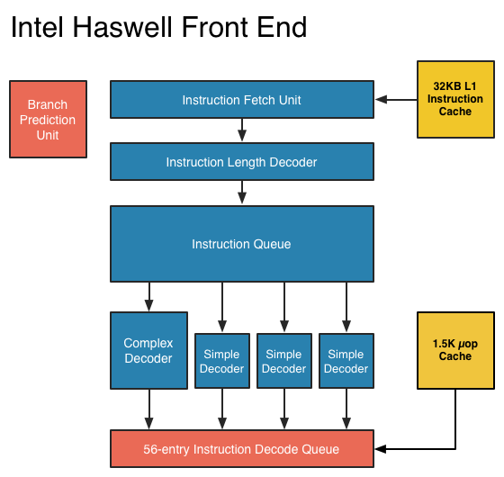
In short, there aren't many major, high-level changes to see here. Instructions are fetched at the top, sent through a bunch of steps before getting to the decoders where they're converted from macro-ops (x86 instructions) to an internally understood format known to Intel as micro-ops (or µops). The instruction fetcher can grab 4 - 5 x86 instructions at a time, and the decoders can output up to 4 micro-ops per clock.
Sandy Bridge introduced the 1.5K µop cache that caches decoded micro-ops. When future instruction fetch requests are made, if the instructions are contained within the µop cache everything north of the cache is powered down and the instructions are serviced from the µop cache. The decode stages are very power hungry so being able to skip them is a boon to power efficiency. There are also performance benefits as well. A hit in the µop cache reduces the effective integer pipeline to 14 stages, the same length as it was in Conroe in 2006. Haswell retains all of these benefits. Even the µop cache size remains unchanged at 1.5K micro-ops (approximately 6KB in size).
Although it's noted above as a new/changed block, the updated instruction decode queue (aka allocation queue) was actually one of the changes made to improve single threaded performance in Ivy Bridge.
The instruction decode queue (where instructions go after they've been decoded) is no longer statically partitioned between the two threads that each core can service.
The big changes in Haswell are at the back end of the pipeline, in the execution engine.


245 Comments
View All Comments
Penti - Saturday, October 6, 2012 - link
Also FPU/SIMD has been a large part in later ARM designs and implementations. It's really a big deal as we saw with the chips lacking some of those parts. You shouldn't forget how important those bits are. Others have failed because they didn't take it seriously. That was 15-20 years ago even. Doesn't mean they are yet fighting x86-64 chips in high-end servers and workstation though. We will certainly see them entering that market by 2015 though.Arbee - Friday, October 5, 2012 - link
Cortex A9's big IPC improvement came from going out-of-order, which kind of ruins your argument.Similarly, the X360/PS3 PowerPC chips are strict in order and super ultra slow as a result - at 3.2 GHz they can't match a PowerMac G5 with out-of-order at 2.2 GHz. But I suspect that wasn't the point - Sony and MS can claim the eye-popping (in 2006) 3.2 GHz figure, and the heat production is certainly less than a PPC G5.
wumpus - Friday, October 5, 2012 - link
Has anyone seen an A9 in the wild? I don't doubt huge IPC improvements (back when O-O-O was new, it tended to double performance). My statement is that it will kill GIPS/W and that Intel can much more easily design a chip that can beat it in both raw performance and GIPS/W (note that your mention of heat production agrees with me).Also note I suspect that the goal of A9 is to keep the power low enough to keep it out of where Intel wants to go. A rough guess is that ARM might have a chance with dual issue o-o-o, but past that (roughly where Pentium Pro was designed) they can't really go.
ElvenLemming - Friday, October 5, 2012 - link
The Cortex A9 has been in most major phone/tablet SoCs for the past two or so years. Apple's A5, A5X; Samsung's Exynos 4210, 4212, 4412; TI's OMAP 4 series; Nvidia's Tegra 2 and 3.Cortex A15 is probably what you were thinking of that we've yet to see out in the wild. It's out-of-order like the A9, but with a great deal of other improvements.
ericore - Friday, October 5, 2012 - link
Currently AMD has the upper hand on the notebook segment on battery life. Haswell changes that, but as is always the case with Intel, they will be pricey. And that's why AMD will still have 50% of the market because vendors are cheap.Power savings are much less relevant on desktop front; I don't care so much about power as i do of heat. AMD X4 700, ship an awsome 4 core cpu for 75$. Technically, it has all that you need from a CPU. Add a Radeon 7770 (again cheap) and your golden. Ya Intel is faster, but both Intel and Nvidia have shitty low end products and that's even more true when you think of atom. 5-15% single threaded performance is not anything that is going to burry AMD lol.
On top of that, AMD has an atom KILLER, a contracts with all major console vendors.
Haswell will have surprisingly little impact on AMD; what I am saying is if you look at your own expectations, you'll realize they were highly inflated and you'll wonder why it didn't do more damage to AMD. I've explained the why. Nevertheless broadwell is a significant threat, and we'll probably see AMD start to lose market share (much more than with haswell) unless AMD can fight back and it will; but nobody knows if it will be enough.
A5 - Friday, October 5, 2012 - link
Uh, wow.Zink - Saturday, October 6, 2012 - link
http://www.tomshardware.com/reviews/gaming-cpu-rev...tipoo - Friday, October 5, 2012 - link
"Overall performance gains should be about 2x for GT3 (presumably with eDRAM) over HD 4000 in a high TDP part."Does this mean the regular GT3 without eDRAM cache will be twice the performance of the HD4000 and the one with the cache will be 4x? Or that the one with the cache will be 2x? In which case, what would the one with no cache perform like, with so many more EUs the first is probably correct, right?
tipoo - Friday, October 5, 2012 - link
"presumably with eDRAM"...So the GT3 in Haswel has over double the EUs of Ivy Bridge, but without the cache it doesn't even get to 2x the performance? Seems off to me, doesn't it seem like the GT3 on its own would be 2x the performance while the eDRAM cache would make for another 2x?DanNeely - Saturday, October 6, 2012 - link
It probably means that, like AMD, Intel is hitting the wall on memory bandwidth for IGPs. When it finally arrives, DDR4 will shake things up a bit; but DDR3 just isn't fast enough.