Intel's Haswell Architecture Analyzed: Building a New PC and a New Intel
by Anand Lal Shimpi on October 5, 2012 2:45 AM ESTDecoupled L3 Cache
With Nehalem Intel introduced an on-die L3 cache behind a smaller, low latency private L2 cache. At the time, Intel maintained two separate clock domains for the CPU (core + uncore) and a third for what was, at the time, an off-die integrated graphics core. The core clock referred to the CPU cores, while the uncore clock controlled the speed of the L3 cache. Intel believed that its L3 cache wasn't incredibly latency sensitive and could run at a lower frequency and burn less power. Core CPU performance typically mattered more to most workloads than L3 cache performance, so Intel was ok with the tradeoff.
In Sandy Bridge, Intel revised its beliefs and moved to a single clock domain for the core and uncore, while keeping a separate clock for the now on-die processor graphics core. Intel now felt that race to sleep was a better philosophy for dealing with the L3 cache and it would rather keep things simple by running everything at the same frequency. Obviously there are performance benefits, but there was one major downside: with the CPU cores and L3 cache running in lockstep, there was concern over what would happen if the GPU ever needed to access the L3 cache while the CPU (and thus L3 cache) was in a low frequency state. The options were either to force the CPU and L3 cache into a higher frequency state together, or to keep the L3 cache at a low frequency even when it was in demand to prevent waking up the CPU cores. Ivy Bridge saw the addition of a small graphics L3 cache to mitigate this situation, but ultimately giving the on-die GPU independent access to the big, primary L3 cache without worrying about power concerns was a big issue for the design team.
When it came time to define Haswell, the engineers once again went to Nehalem's three clock domains. Ronak (Nehalem & Haswell architect, insanely smart guy) tells me that the switching between designs is simply a product of the team learning more about the architecture and understanding the best balance. I think it tells me that these guys are still human and don't always have the right answer for the long term without some trial and error.
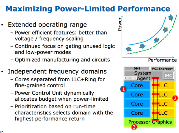
The three clock domains in Haswell are roughly the same as what they were in Nehalem, they just all happen to be on the same die. The CPU cores all run at the same frequency, the on-die GPU runs at a separate frequency and now the L3 + ring bus are in their own independent frequency domain.
Now that CPU requests to L3 cache have to cross a frequency boundary there will be a latency impact to L3 cache accesses. Sandy Bridge had an amazingly fast L3 cache, Haswell's L3 accesses will be slower.
The benefit is obviously power. If the GPU needs to fire up the ring bus to give/get data, it no longer has to drive up the CPU core frequency as well. Furthermore, Haswell's power control unit can dynamically allocate budget between all areas of the chip when power limited.
Although L3 latency is up in Haswell, there's more access bandwidth offered to each slice of the L3 cache. There are now dedicated pipes for data and non-data accesses to the last level cache.
Haswell's memory controller is also improved, with better write throughput to DRAM. Intel has been quietly telling the memory makers to push for even higher DDR3 frequencies in anticipation of Haswell.


245 Comments
View All Comments
CaptainDoug - Friday, October 5, 2012 - link
Quite the read. Very informational. Anandtech has some of the best tech writers. True online journalism. Sometimes i miss that while reading tech blogs... You guys are a cut above.. at least one.colonelclaw - Friday, October 5, 2012 - link
Couldn't agree more, this article really brightened up what was otherwise a pretty miserable afternoon here in London.When am I going to be able to walk into a shop and buy something with Haswell inside it? Next March maybe?
Kepe - Friday, October 5, 2012 - link
As stated in the article, Haswell is coming in the summer of 2013.linuxlowdown - Saturday, October 6, 2012 - link
Tag team Intel fanboy puke.Azethoth - Sunday, October 7, 2012 - link
How do I downvote stupid crap like this "Tag team Intel fanboy puke." comment so that collectively we can see high quality comments without having to wade through the interturds as well? It really takes away from the best article I have read in a long time. Not because it is about Intel, but because it is about the state of the art.medi01 - Tuesday, October 9, 2012 - link
Well, I'd also ask how do I downvote stupid butt kissing like OP, while we are at rating....Kisper - Saturday, October 20, 2012 - link
Many people enjoy well written and informative articles. Are you telling me that if you wrote, you would not enjoy positive feedback from your readers?CaptainDoug - Tuesday, October 23, 2012 - link
Exactly.actionjksn - Sunday, October 7, 2012 - link
Why are you even on this article dumb fuck? I'm sure there is something that is of interest to you on the internet somewhere.medi01 - Tuesday, October 9, 2012 - link
Not sure about him, but I've looked into this article to figure power targets for haswell (especially interesting to compare to ARM crowd), NOT to read orgasmic comments about eternal wizdom of Intel's engineering...