Samsung SSD 840 (250GB) Review
by Kristian Vättö on October 8, 2012 12:14 PM EST- Posted in
- Storage
- SSDs
- Samsung
- TLC
- Samsung SSD 840
Lower Endurance—Why?
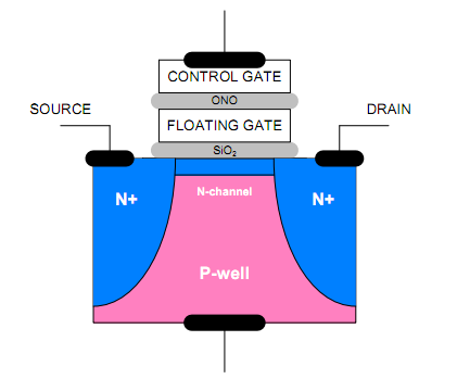
Below we have a diagram of a MOSFET (Metal Oxide Semiconductor Field Effect Transistor). When programming a cell, voltage is placed on the control gate, which forms an electric field that allows electrons to tunnel through the silicon oxide barrier to the floating gate. Once the tunneling process is complete, voltage to the control gate is dropped back to 0V and the silicon oxide acts as an insulator. Erasing a cell is done in a similar way but this time the voltage is placed on the silicon substrate (P-well in the picture), which again creates an electric field that allows the electrons to tunnel through the silicon oxide.
While the MOSFET is exactly the same for SLC, MLC and TLC, the difference lies in how the cell is programmed. With SLC, the cell is either programmed or it's not because it can only be "0" or "1". As MLC stores two bits in one cell, its value can either be "00", "01", "10" or "11", which means there are four different voltage states. TLC ups the voltage states to eight as there are eight different combinations of "0" and "1" when grouped in groups of three bits. Below are diagrams showing the graphical version of the voltage states:
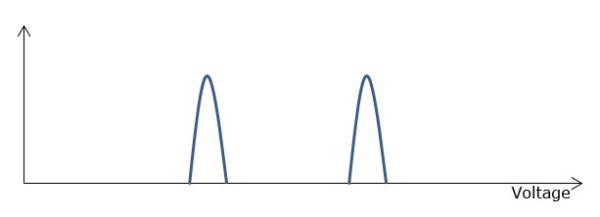
SLC
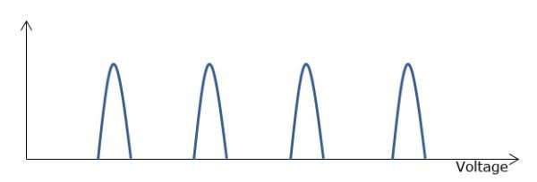
MLC
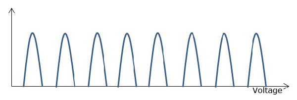
TLC
The above diagrams show the voltages for brand new NAND—everything looks nice and neat and the only difference is that TLC has more states. However, the tunneling process that happens every time the cell is programmed or erased wears the silicon oxide out. The actual oxide is only about 10nm thick and it gets thinner every time a smaller process node is introduced, which is why endurance gets worse as we move to smaller nodes. When the silicon dioxide wears out, atomic bonds break and some electrons may get trapped inside the oxide during the tunneling process. That builds up negative charge in the silicon oxide, which in turn negates some of the control gate voltage when the cell is programmed.
The wear results in longer erase times because higher voltages need to be applied for longer times before the right voltage is found. Remember, the controller can't adjust to changes in program and erase voltages (well, some can; more on this on the next page) that come from the trapped electrons, cell leakage, and other sources. If the voltage that's supposed to work doesn't, the controller has to basically go on guess basis and simply try different voltages before the right one is found. That takes time and causes even more stress on the silicon oxide.
The difference between SLC, MLC, and TLC is pretty simple: SLC has the fewest voltage states and hence it can tolerate bigger changes in voltages. With TLC, there are eight different states and hence a lot less voltage room to play with. While the exact voltages used are unknown, you basically have to divide the same voltage into eight sections instead of four or two like the graphs above show, which means the voltages don't have room to change as much. The reason why a NAND block has to be retired is that erasing it starts to take too long, which impacts performance (and eventually a NAND block simply becomes nonfunctional, e.g. the voltage states for 010 and 011 begin to overlap).
There is also more and more ECC needed as the NAND wears out because the possibility for errors is greater. With TLC, that's once again a bigger problem because there are three bits to correct instead of one or two. While today's ECC engines are fairly powerful, at some point it will be easier to just retire the block than to keep correcting errors.


86 Comments
View All Comments
JarredWalton - Monday, October 8, 2012 - link
What price are you looking at? The table shows $199.99 for the 250GB Samsung 840 (MSRP) and $249.99 for the 256GB Samsung 840 Pro.Kevin G - Monday, October 8, 2012 - link
On the fourth page:"With perfect wear-leveling and write amplification of 1x, you would get 256TiB of writes out of a 250GB Samsung 840 with TLC NAND and 1,000 P/E cycles. "
Shouldn't it be 256 GiB?
JarredWalton - Monday, October 8, 2012 - link
No; he's accounting for the visible storage capacity (and spare area). So 250GB is 256GiB of NAND but only 250GB end-user storage. You can still write 256TiB of data (256GiB * 1000 P/E), which means on a 250GB SSD you end up with the ability to write 281TB of data (for an effective P/E cycles of 1125).schizoide - Monday, October 8, 2012 - link
I'm not comfortable with TLC, particularly since it doesn't come at a huge absolute cost savings. I've been burned too often with SSDs, and now only buy the most bulletproof devices available. Maybe next generation. Maybe.Death666Angel - Tuesday, October 9, 2012 - link
I wouldn't draw any conclusion for pricing just yet. Everyone is comparing street prices of current gen SSDs to MSRP of next gen SSDs. Give it a few months to get the 840 into stores and selling and then we'll se how prices fair.I'm personally fairly confident that there will be a distinct cost advantage.
name99 - Tuesday, October 9, 2012 - link
Have ANY SSDs given you a failure based on the flash cells themselves, rather than on crappy firmware?It's stupid to demonize a technology because some companies sold you a bad product --- especially when your response is to refuse to buy a product from a company that is known (in this respect at least) NOT to have shipped crappy firmware.
harijan - Monday, October 8, 2012 - link
Pretty sure 3650GiB != 3.65TiB.3650GB == 3.65TB.
It doesn't do anything to your percentages, but this is Anandtech, we hold you to higher standards ;)
Kristian Vättö - Tuesday, October 9, 2012 - link
You are correct, I forgot that binary units don't scale up linearly (1000GiB is not 1TiB); metrics are just so much simpler. Thanks for the heads up, I've fixed the math now.iaco - Monday, October 8, 2012 - link
I wonder if Samsung will ever make a SSD made of SLC NAND. The performance would be amazing.Conficio - Monday, October 8, 2012 - link
First thanks to the Kristan and the Anand Team for another comprehensive review and the inclusion of in depth knowledge about the technology behind it.I'd like to see included in the test (or in another article) a review of the available tools for each SSD. I think it is important to know if the manufacturer supports its tools to low level format, secure erase, TRIM, ROM update etc. beyond the obligatory Windows (7). Are those available for Linux (command line and/or GUI)? Are they available for Mac OSX? Do they work if the drive is connected over USB? Are these tools user friendly to use?
It is useless if I buy an SSD and have to find out that Mac OSX does not support the tools. I have a couple of Vertex drives which I can't find a way to secure erase in order to restore full performance. They are pre TRIM drives and Mac OS X does not support trim on them anyway.
As with motherboards, the the BIOS or UEFI is important, so is with SSDs the ability to actually perform some of the low level functions. I hope you can add that to your workload! A comparison of the different tools for each manufacturer for current drives would be a great start. Thanks again!