The iPhone 5's A6 SoC: Not A15 or A9, a Custom Apple Core Instead
by Anand Lal Shimpi on September 15, 2012 2:15 PM EST- Posted in
- Smartphones
- Apple
- Mobile
- SoCs
- iPhone 5
The A6 GPU: PowerVR SGX 543MP3?
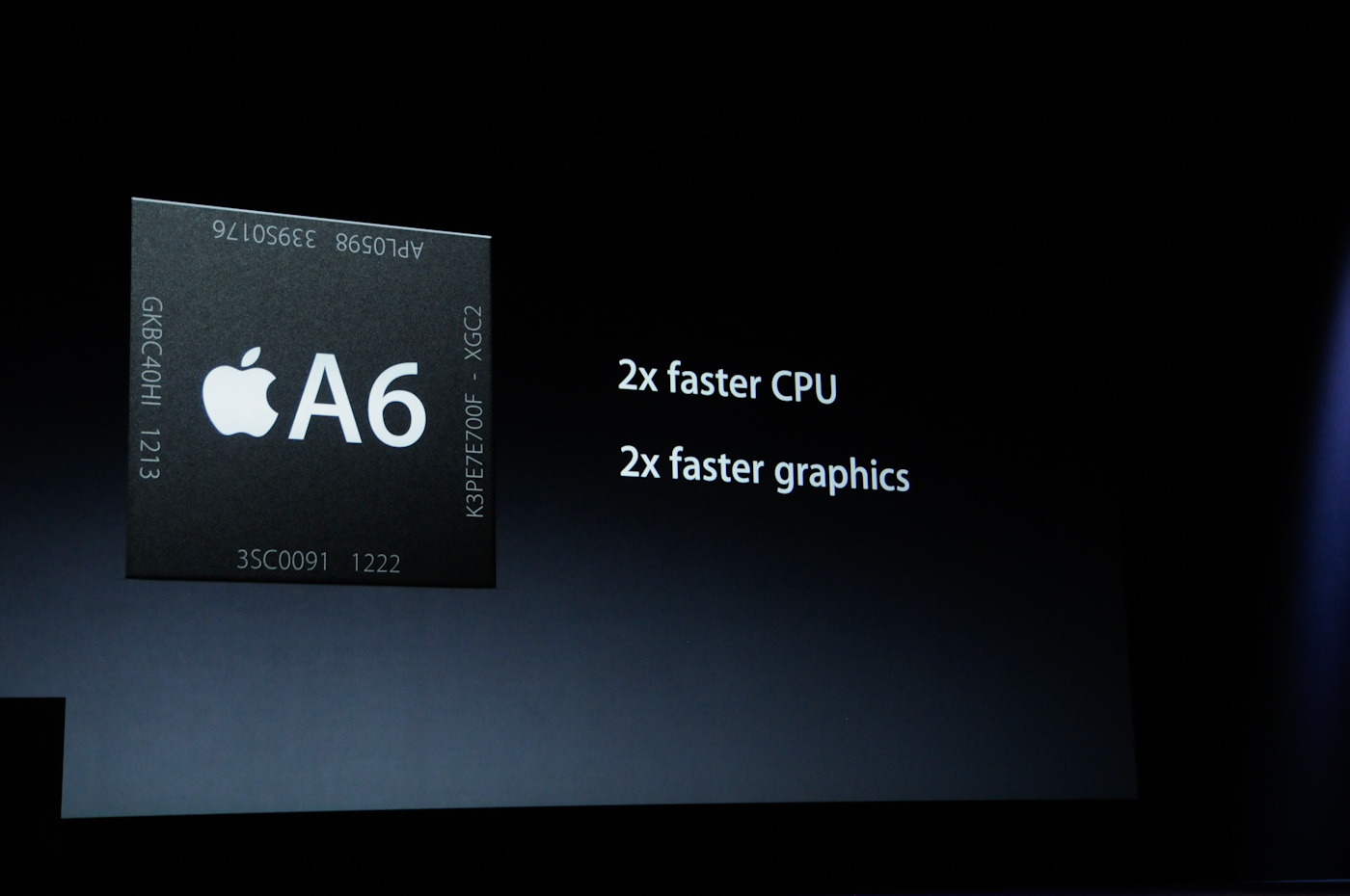
Apple made a similar "up to 2x" claim for GPU performance. It didn't share any benchmarks, but there are four options here:
1) PowerVR SGX 543MP2 (same as in A5) at 2x the clock speed
2) PowerVR SGX 543MP4 at the same clock as the MP2 in the A5
3) Marginally higher clocked PowerVR SGX 543MP3
4) Next-gen PowerVR Rogue GPU
It's too early for #4. The first option makes sense but you run into the same issues as on the CPU side with higher voltages used to ramp clocks up (also possible that you drop voltages in the move to the new process technology).
The second option trades voltage for die area, which based on the A5X Apple is clearly willing to spend where necessary.
The third is sort of the best of both worlds. You don't take a huge die area penalty and at the same time don't run at a significantly higher frequency, and you can get to that same 2x value.
The third option is the most elegant and likely what Apple chose here. Remember that overall die size is dictated by the amount of IO you have around the chip. The A5X had four 32-bit LPDDR2 memory controllers, which gave Apple a huge die area to work with. The move to a smaller manufacturing process cuts down the total die area, which means Apple would either have to add a ton of compute (to fill empty space, no sense in shipping a big chip with a bunch of unused area) or reduce the memory interface to compensate. Pair that knowledge with the fact that Apple doesn't have the same memory bandwidth requirements on the iPhone 5 (0.7MP vs. 3.1MP display) and it makes sense that Apple would go for a narrower memory interface with the A6 compared to the A5X.
How much narrower? Phil Schiller mentioned the A6 was 22% smaller than the A5. We can assume this is compared to the 45nm A5 and not the 32nm A5r2, which would mean that we don't have any more memory channels compared to the A5. In other words, it's quite likely the A6 has a 2x32-bit LPDDR2 memory interface once again.
Final Words
There's not much more to add for now. We'll have a device in a week and I suspect the first reviews will be out a day or two before then. Then the real work begins on finding out exactly what Apple has done inside the A6. If anyone has been dying to put together some good low level iOS benchmarks, now is the time to start.
This is a huge deal for Apple. It puts the company in another league when it comes to vertical integration. The risks are higher (ARM's own designs are tested and proven across tons of different devices/platforms) but the payoff is potentially much greater. As Qualcomm discovered, it's far easier to differentiate (and dominate?) if you're shipping IP that's truly unique from what everyone else has.
Now we get to see just how good Apple's CPU team really is.


163 Comments
View All Comments
zanon - Saturday, September 15, 2012 - link
Thanks for the write up Anand, this is an interesting step forward and I very much look forward to seeing what they've put together. We've known for years that Apple has been acquiring significant chip design talent (P. A. Semi being a major example), but I think this will be the first time we'll get to see it really put to use at the lowest and most core levels, rather then merely SoC integration or peripheral stuff.It's been many years since we last saw a wide array of companies trying to make different CPUs. It'll be very interesting to see what all comes of it.
chromatix - Saturday, September 15, 2012 - link
I believe they leave gaps in the numbering scheme to allow for new types of cores in lower performance and power consumption brackets.The Cortex-A8 was the first ARMv7-A design. It was followed considerably later by the A5 and A9, offering lower and higher performance (and power consumption) respectively. The A7 and A15 are the latest pair in the same vein.
There are also Cortex-R and Cortex-M series CPUs, following the ARMv7-R and ARMv7-M architectures respectively (except that the Cortex-M0, the very smallest ARM core, follows ARMv6-T2 instead). These designs are for Realtime and eMbedded designs respectively and have appropriate design tradeoffs accordingly.
None of these are to be confused with the ARM7 core, which dates back to the mid-1990s (using ARMv4T architecture) and is still insanely popular because it uses only a few ten-thousands of transistors. It has been regularly updated to work with newer processes, so these days it is a complete CPU core in a tiny fraction of a square millimetre, and runs at several hundred MHz. All together now: "Imagine a Beowulf cluster of those!"
KPOM - Saturday, September 15, 2012 - link
After you are done wiping the egg off your face from your proud tweets earlier this week that it was an A15, I'm assuming you'll be running some tests once you get your hands on an iPhone 5. Is that a good assumption?It will be interesting to see how well this compares to the A15, and what competitors will put into their phones over the coming months.
DigitalFreak - Saturday, September 15, 2012 - link
DickSufo - Sunday, September 16, 2012 - link
Oh my, what buffoons. Factually inaccurate tweets? However will they live it down? *snicker*ltcommanderdata - Saturday, September 15, 2012 - link
The SGX554MP2 is also a possibility. It offers 2x the ALU performance of the SGX543MP2, equivalent to the SGX543MP4 without doubling the TMU or ROP count which isn't as necessary given the resolution difference between the 2012 iPad and iPhone 5. Apple may not want to introduce a new GPU core when Rogue is around the corner though.Is it too early for 2x32-bit LPDDR3? Sticking with LPDDR2 they could only move from LPDDR2-800 in the A5 to LPDDR2-1066, which is a pretty marginal difference in bandwidth to feed a 2x faster CPU and particularly a 2x faster GPU. If they could get LPDDR3-1600, they could match A5X memory bandwidth with half the memory controllers.
Any speculation on cache sizes? Shipping Cortex A9 designs seem to have stuck with 512KB per core, which was unchanged from higher-end Cortex A8 designs. Since Apple isn't worried about die space, would moving to 1MB L2 cache per core be worthwhile? Intel pushed a large, low latency L2 cache in Dothan as a power efficient way to increase performance so there is merit to that approach. Would Apple consider a shared L3 cache like Sandy Bridge/Ivy Bridge to share data between the CPU and GPU?
Alexvrb - Sunday, September 16, 2012 - link
I have to admit, I was sure it was an MP4 like the latest iPad... but I hadn't considered the possibility of an MP3 (at slightly higher clocks than their A5 used) or an SGX554. I hadn't seen or heard of 554 being used, so I sort of forgot the design was there. Waiting.Won't be long until Series 6 though, which will produce some pretty amazing mobile graphics. :D
erple2 - Sunday, September 16, 2012 - link
Doesn't the Archos 101sx use the omap 4470, and the sgx 554? I seem to remember reading that in the review on this very site (page 3, middle of second paragraph).Alexvrb - Sunday, September 16, 2012 - link
I'm pretty sure that the 4470 has an SGX544. Looking around it looks like there were rumors of it being an SGX554 before release, but those same rumors said the CPU cores would be clocked at 1.8Ghz. So... yeah.dagamer34 - Saturday, September 15, 2012 - link
This makes a lot more sense than Apple having A15 CPUs (I always found it a little weird that Apple would be ready with them before TI when they were it's lead development partner, and we haven't seen silicon at final clocks yet).Invariably, if we've got a custom CPU core, then sooner or later we're going to get a custom GPU core and the Apple SoC is going to be a black box where the only data we get about it is from benchmarks.
I'm glad the mistake has been cleared up and eager to see how it performs against Krait and Cortex A15.