Intel Haswell Architecture Disclosure: Live Blog
by Anand Lal Shimpi on September 11, 2012 1:27 PM EST- Posted in
- IT Computing
- CPUs
- Intel
- Haswell
- Trade Shows
- IDF 2012
02:28PM - And we're done! We'll be working on a deeper Haswell architecture piece over the next couple of days.
02:27PM - Intel isn't disclosing exact details on what aspects of voltage regulation have been integrated
02:27PM - But lots of the fine grained control on client Haswell platforms we'll see in servers
02:27PM - Not going into detail on the Haswell server product today
02:27PM - Haswell will include far more power gates on the platform level
02:26PM - Haswell integrates some but not all of the voltage regulation so Intel can do more fine grained control of the pieces inside the die
02:25PM - Sidenote: it's always hilarious to see how many Intel OEMs and competitors end up in these tech insight sessions
02:25PM - TSX support coming in Linux and Windows
02:23PM - Time for Q&A
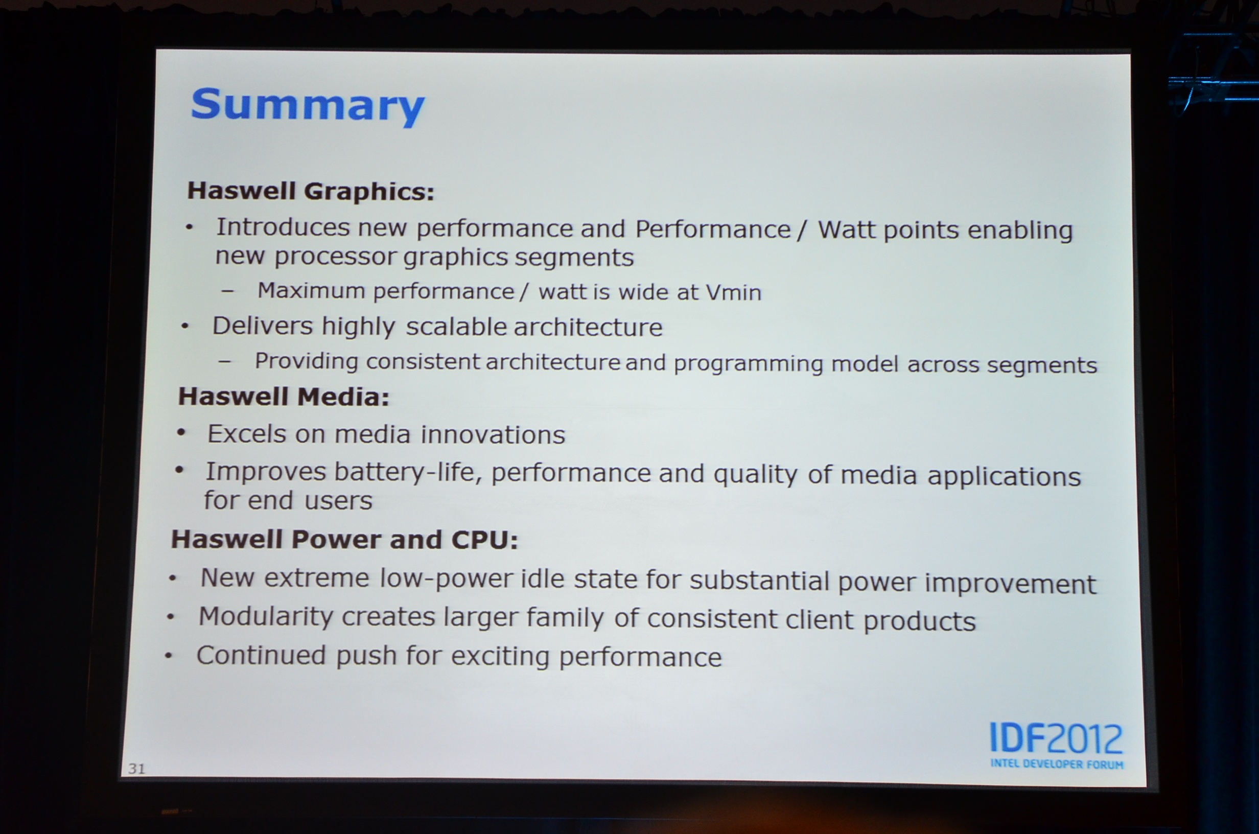
02:22PM - Piazza on Haswell GPU: "this is certainly not the end"
02:21PM - Nearing the end - Summary time

02:21PM - In the past only had two concurrent engines: codec and imaging/scale/composite, now you can do more in parallel as long as there's enough bandwidth to sustain
02:20PM - Now there are three concurrent video engines: codec, imaging and scale/composition
02:19PM - Hardware image stabilization is new in Haswell
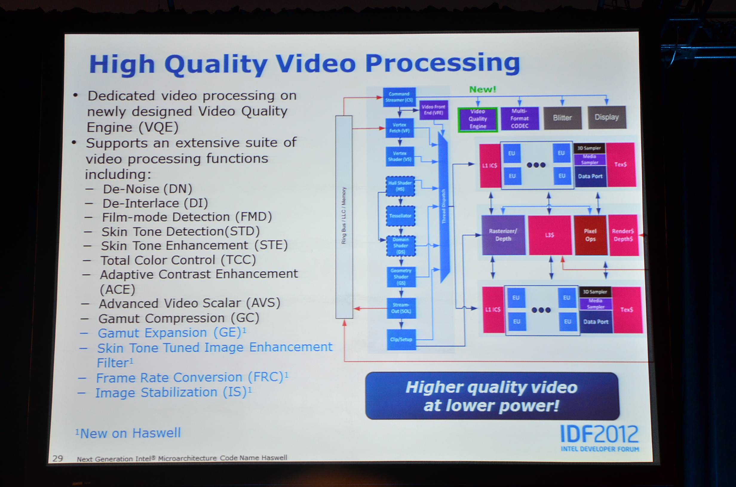
02:18PM - Moved some video processing stuff off the EU array into a dedicated video quality engine
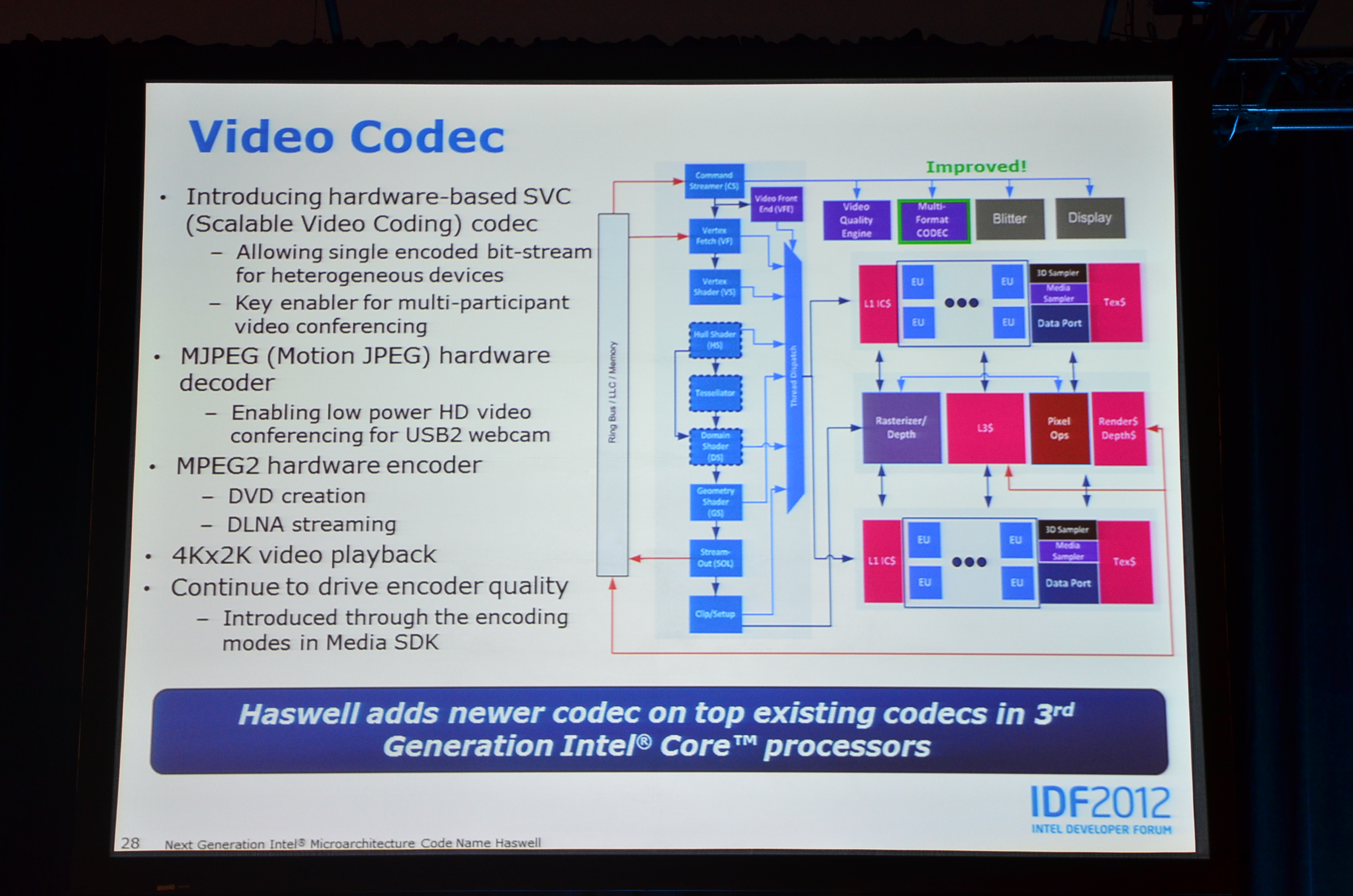
02:15PM - 4Kx2K video acceleration is supported
02:15PM - Usages: video serving, multi-party video conferencing
02:14PM - Introducing hardware based SVC codec, can encode once and playback at multiple resolutions
02:13PM - Higher encode quality, faster Quick Sync with GT3
02:13PM - Now talking about Haswell video processing
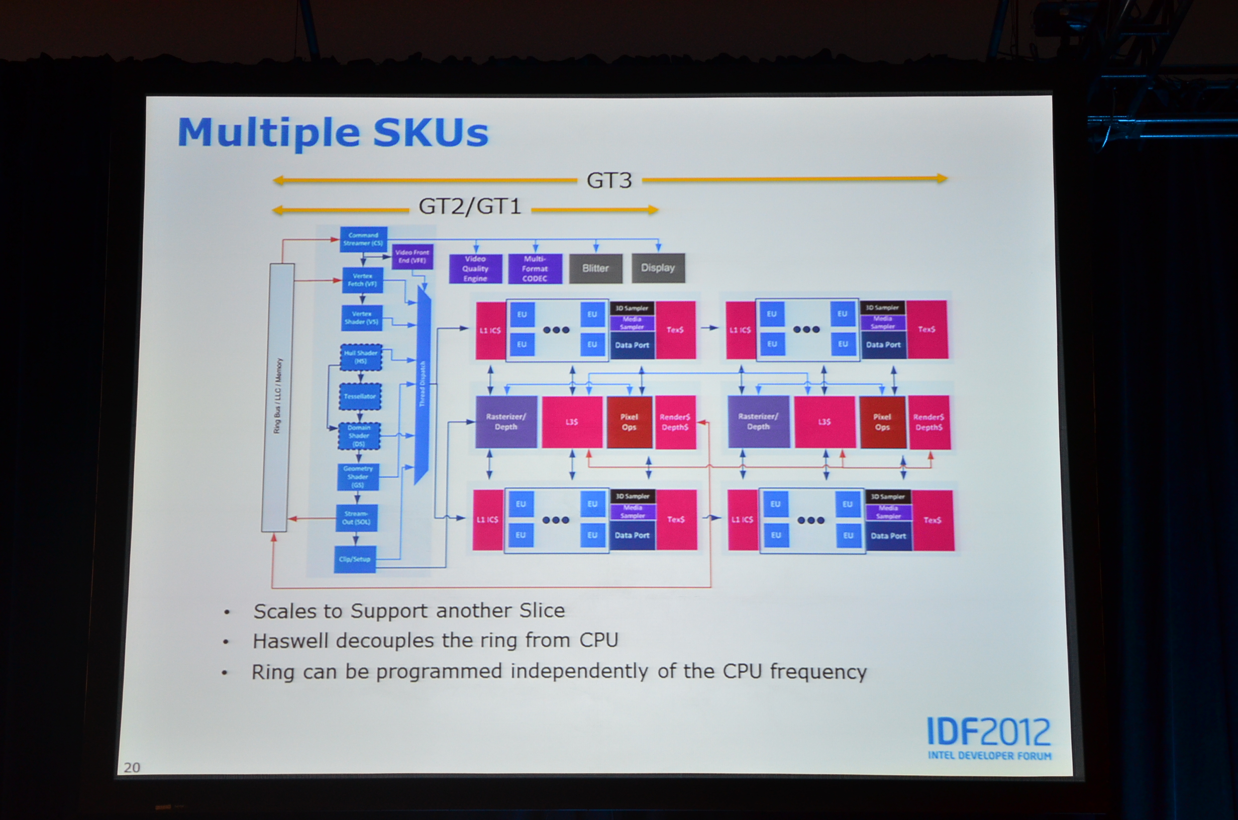
02:11PM - GT3 seems to double everything
02:11PM - Half a terabyte of internal bandwidth between compute and cache
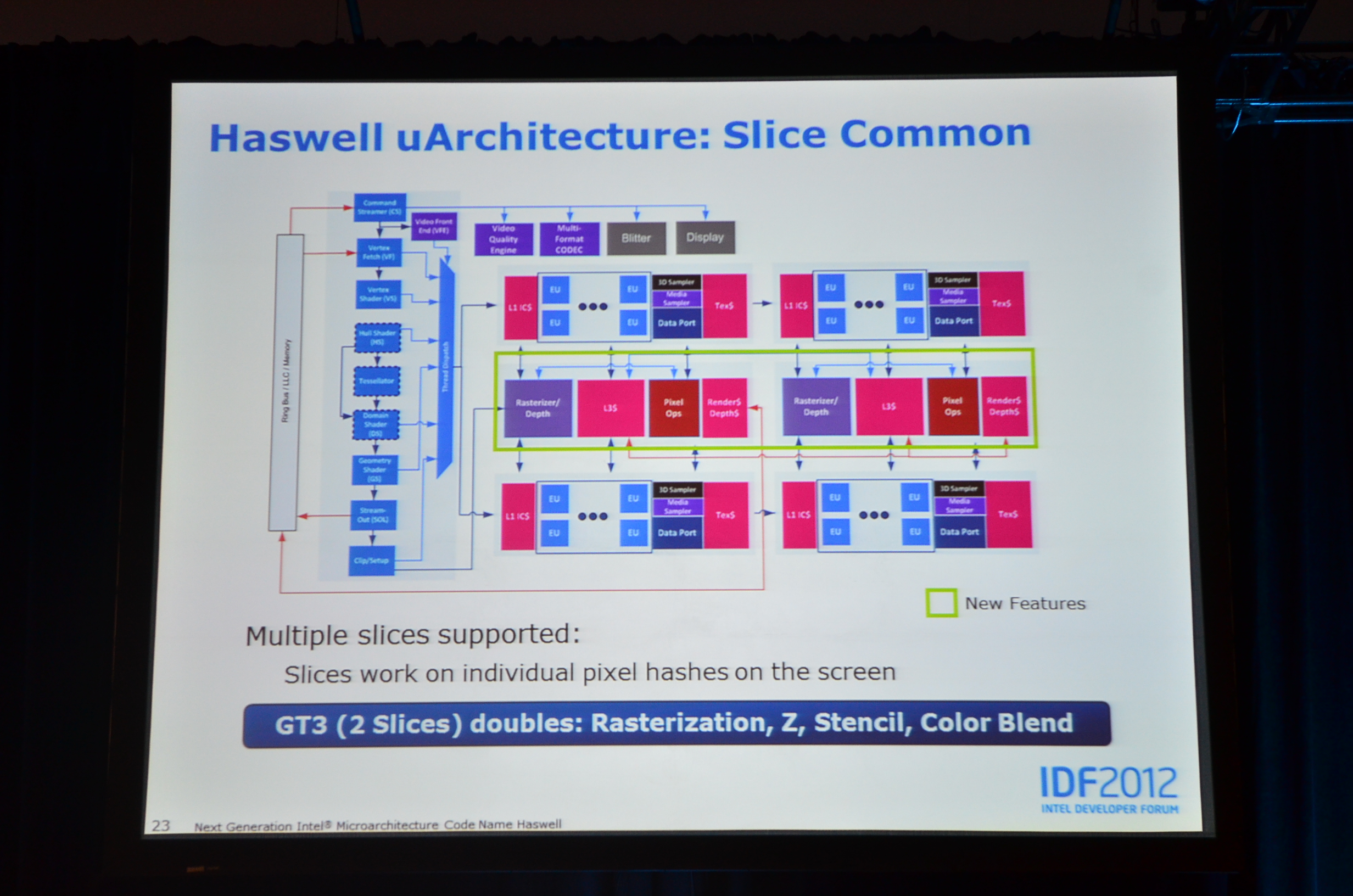
02:10PM - Doubled the performance of most of the fixed function units for normal rendering on the GT3 part
02:09PM - Added a resource streamer at the front end, offloads some driver work which helps the CPU go to sleep so the GPU can do work on behalf of the driver instead of the CPU
02:08PM - Independent voltage/frequency domains for CPU, ring and GPU now?
02:08PM - CPUs can run at low voltage/low frequency, but the GPU can now pull the ring up to feed the engines without pulling up the CPU voltage/frequency
02:08PM - Haswell totally decouples the ring from the CPU
02:08PM - There's now a GT3 part

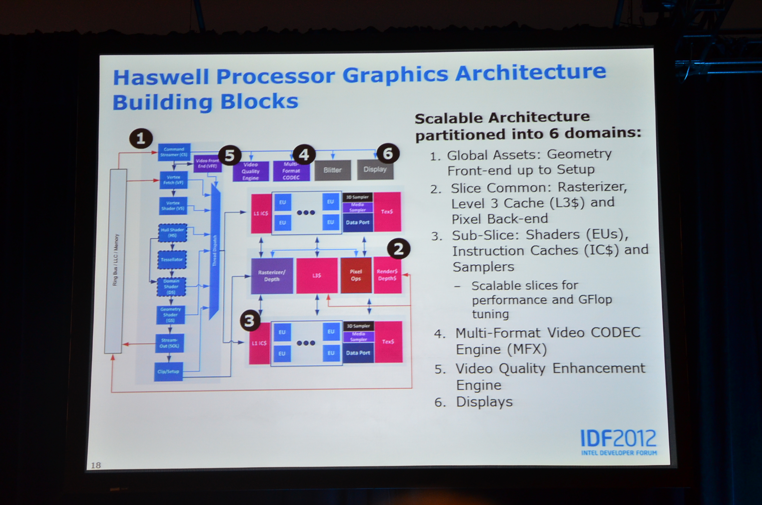
02:07PM - Haswell GPU architecture is similar to IVB, Broadwell will likely be different
02:05PM - Tom Piazza is on the stage
02:04PM - Now on to graphics innovations
02:04PM - One hour session tomorrow on TSX, hmm I hope it doesn't conflict with another major event...
02:03PM - Hardware can then attempt to extract parallelism with concurrent memory accesses
02:03PM - TSX allows the developer to give hints about concurrent accesses
02:03PM - But what if you have two threads accessing the same table but are updating completely independent things?
02:02PM - Normally when you have many cores working on the same data structure, you typically have one thread handle updates and lock the structure for everything else
02:01PM - Now talking about Intel Transactional Synchronization Extensions (TSX)
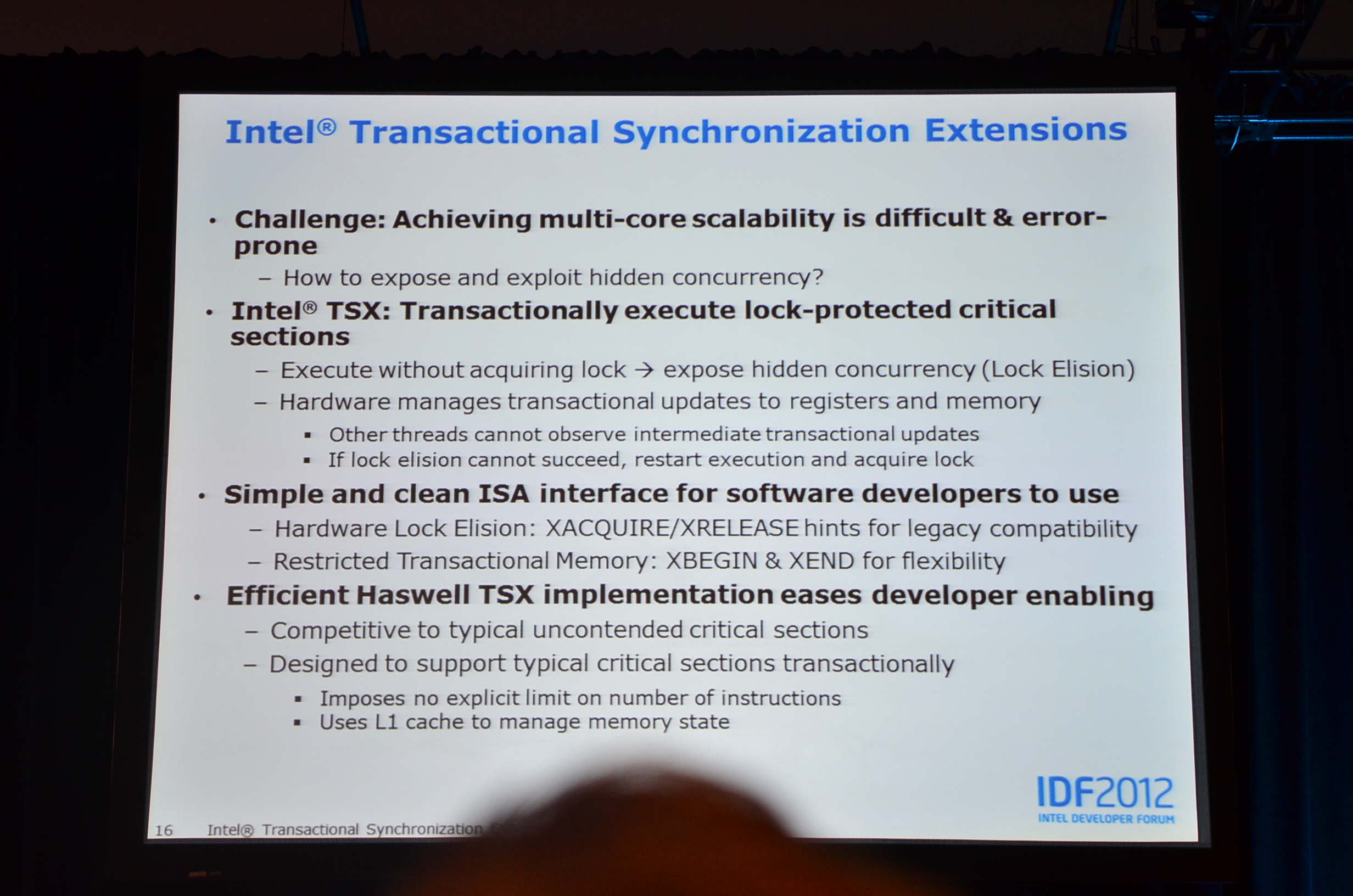
02:01PM - This will benefit AVX2 code as well as on legacy code as well
02:01PM - Also doubled bandwidth at L2 cache, went from 1 read of the L2 every other clock cycle to a read every clock cycle
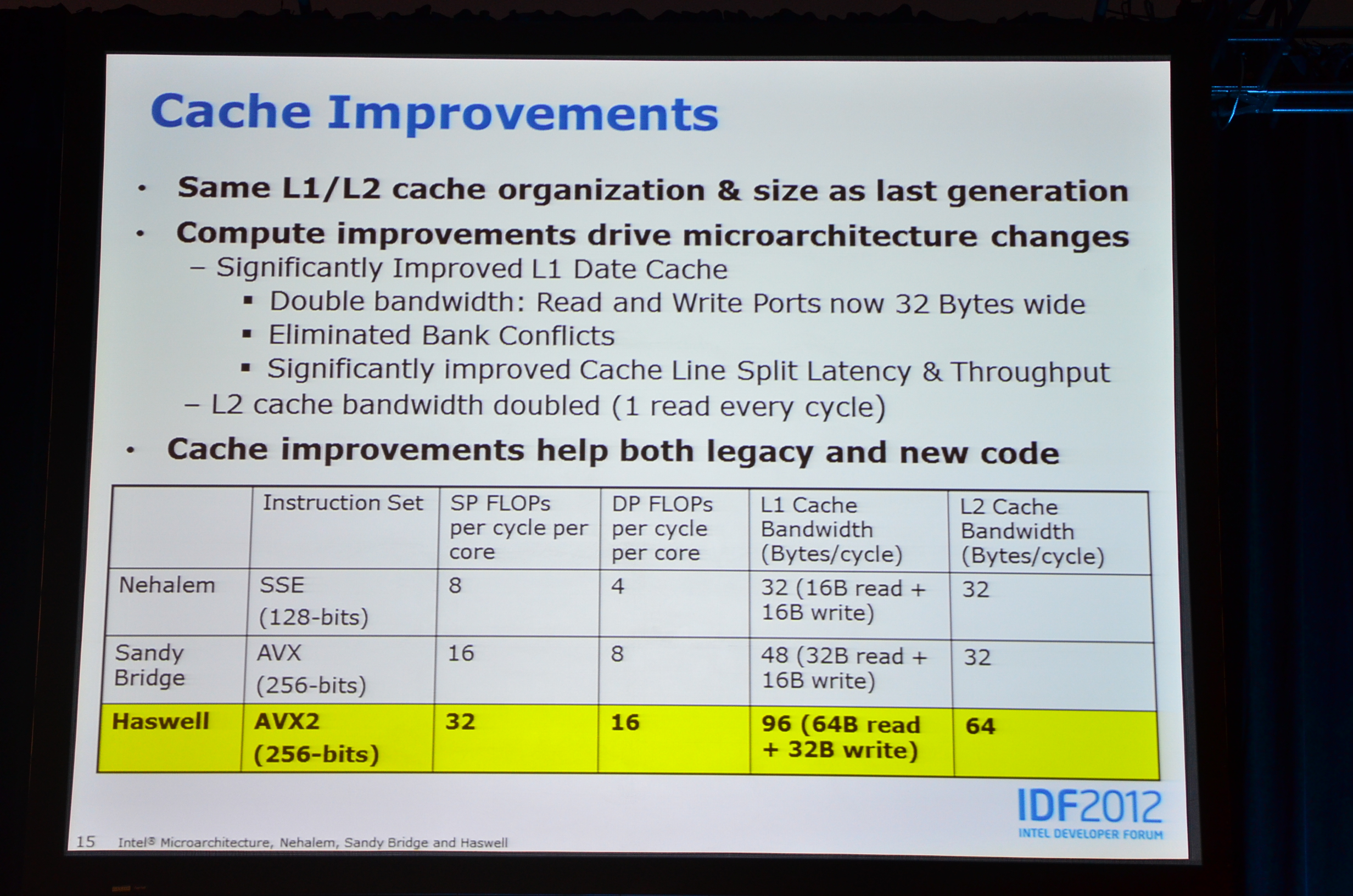
01:59PM - This is for the L1 data cache
01:59PM - Can also do a write of the cache as well, 2 reads + 1 write at 256bits wide
01:59PM - Can now do a 256-bit load, AVX load, with a single read of the cache - and two ports
01:58PM - Same sizes L1/L2 caches as SNB/IVB
01:58PM - Whenever we double the FLOPS like we did here, you need to double the capability to feed those units
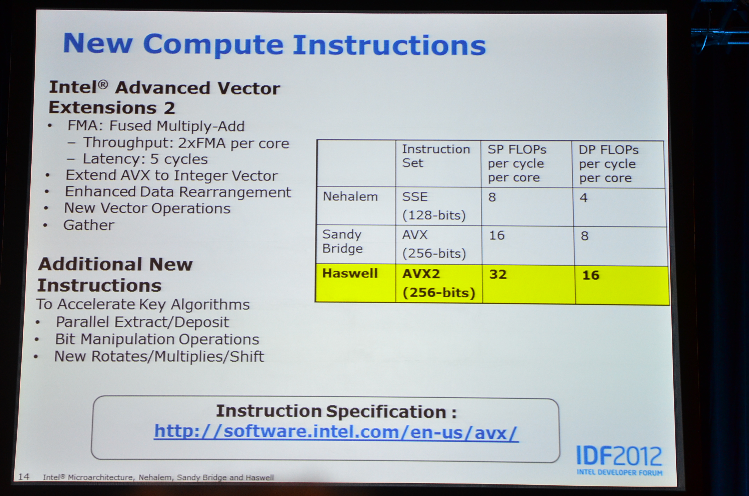
01:57PM - A bunch of new vector and scalar instructions
01:56PM - 4x the peak FP throughput of Nehalem
01:56PM - Since Haswell can do 2 FMAs every cycle per core
01:55PM - AVX2 doubles peak FP throughput of Haswell
01:54PM - Ooh: even deeper dive on Haswell microarchitecture later today
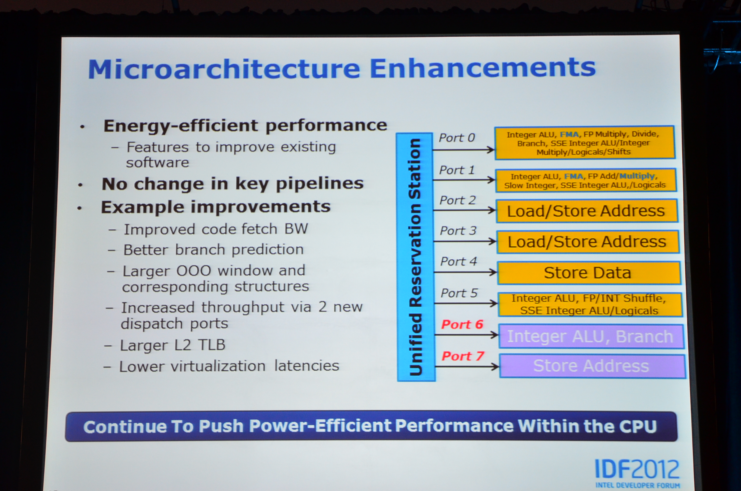
01:54PM - L2 TLB is bigger
01:53PM - We now have the ability to do two FP multiply-adds every cycle
01:53PM - Added another integer ALU, can now execute 2 branches per cycle, another store address port, can do 2 loads and a store every cycle
01:53PM - Haswell adds port 6 and 7, up to 8 ops every cycle
01:53PM - Nehalem/SNB could execute 6 ops every cycle, port 0 - 5
01:52PM - Improved branch prediction
01:52PM - Increasing size of buffers internally, giving us larger OoO window
01:52PM - Now it's time to talk about Haswell CPU microarchitecture
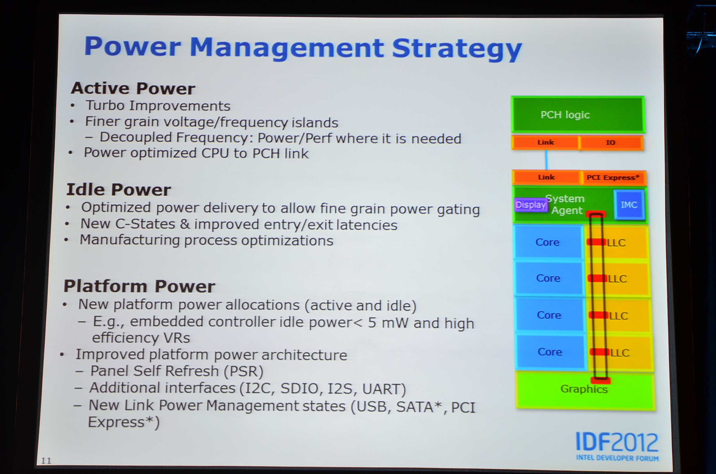
01:51PM - A lot of focus on improving overall platform power, not just the CPU/SoC
01:50PM - Haswell adds more low power IO: I2C, SDIO, I2S, UART
01:50PM - Panel self refresh is supported (if the image doesn't change, display just keeps displaying the same image, rest of the platform goes to sleep)
01:49PM - Worked on increasing efficiency of voltage regulators
01:49PM - To meet the power goals Intel worked with OEMs to give power budgets for main components in the rest of the system
01:48PM - This is how you achieve the 20x platform idle power improvement
01:48PM - We can work with our friends at the process manufacturing side, adapt the process to give us a recipe to fit the processor/die perfectly
01:48PM - Even deeper C-states, can transition between C-states up to 25% faster
01:48PM - Power delivery system is much more fine grained in delivering power to only the pieces that need to be on
01:47PM - That link is optimized for the lowest energy per transfer possible
01:47PM - The link between the CPU and the chipset has been optimized for power, depending on which Haswell part you get
01:47PM - Finer grained voltage/frequency control
01:47PM - Haswell extends the turbo range a little bit
01:46PM - Haswell platform is almost always in this new S0ix active idle state with instant resume
01:45PM - It sounds like Haswell remains in S0 but can quickly transition to active idle, allowing you to get the best of both worlds
01:45PM - "Transparent to well written software"
01:45PM - The hardware does this automatically, continuous, fine grained
01:45PM - Transition times are a lot shorter between high and low power states
01:45PM - This is where we get improvements in platform idle, and battery life
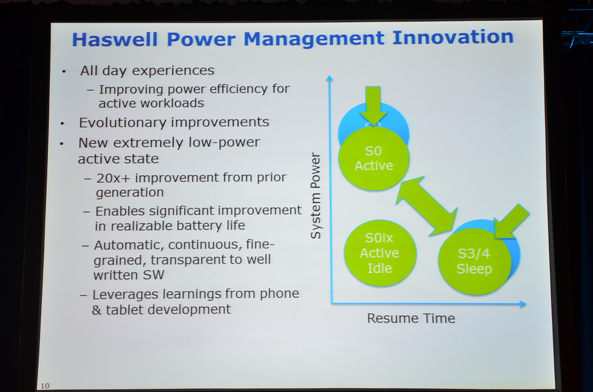
01:44PM - OS thinks the SoC is active, but you get idle power characteristics and can transition between active and idle very quickly
01:44PM - Added completely new set of idle states: S0ix
01:43PM - In the same level of system responsiveness, the system power has come down - transition times to lower power states are quicker now as well
01:43PM - In Haswell, we have worked in making power efficiency/power for active be much better
01:42PM - And you transition between the two, active state was in watts, idle states go into hundreds of milliwatts
01:42PM - IVB had two major power states: S0 (awake) and S3/S4 (sleep)
01:41PM - When you get into those power levels (8W), you can get into very attractive tablets, and also think about going fanless
01:41PM - We can also have the same graphics performance at half the power
01:41PM - Haswell achieves, at the same power level, we have twice the graphics performance [over IVB]
01:40PM - Now talking about Haswell Power Management
01:40PM - "Haswell adds agility"
01:39PM - Active power: from tablet to desktop
01:39PM - Design points in the past still exist, but adding lower power design points that we never had before
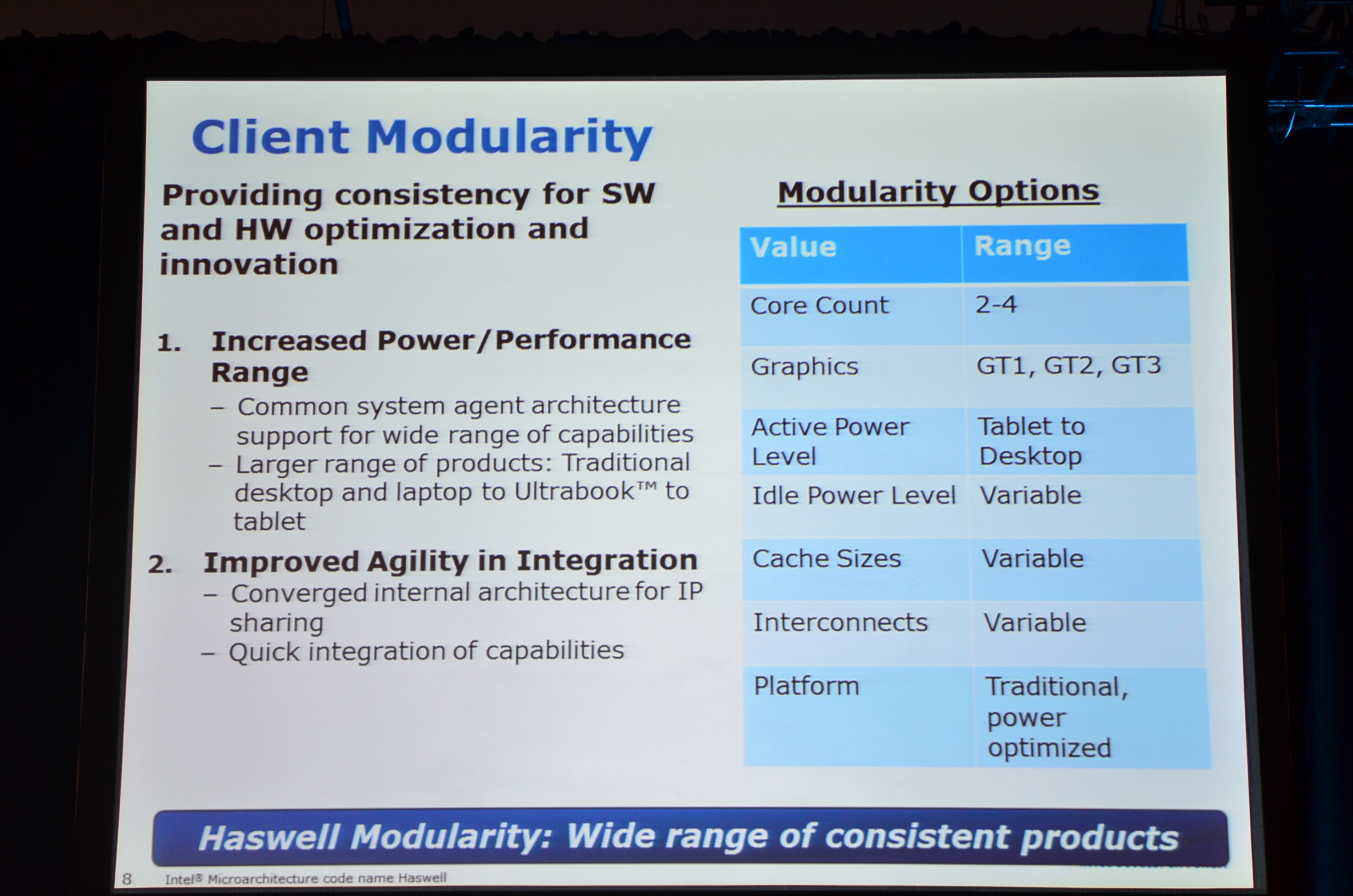
01:38PM - Haswell Modularity: 2 - 4 cores, GT1 - GT3 graphics
01:38PM - The same power enhancements you need to get into tablets actually benefit many core server designs as well
01:35PM - Haswell will go from tablets to servers and everything in between
01:35PM - Today's disclosure will focus on what's new
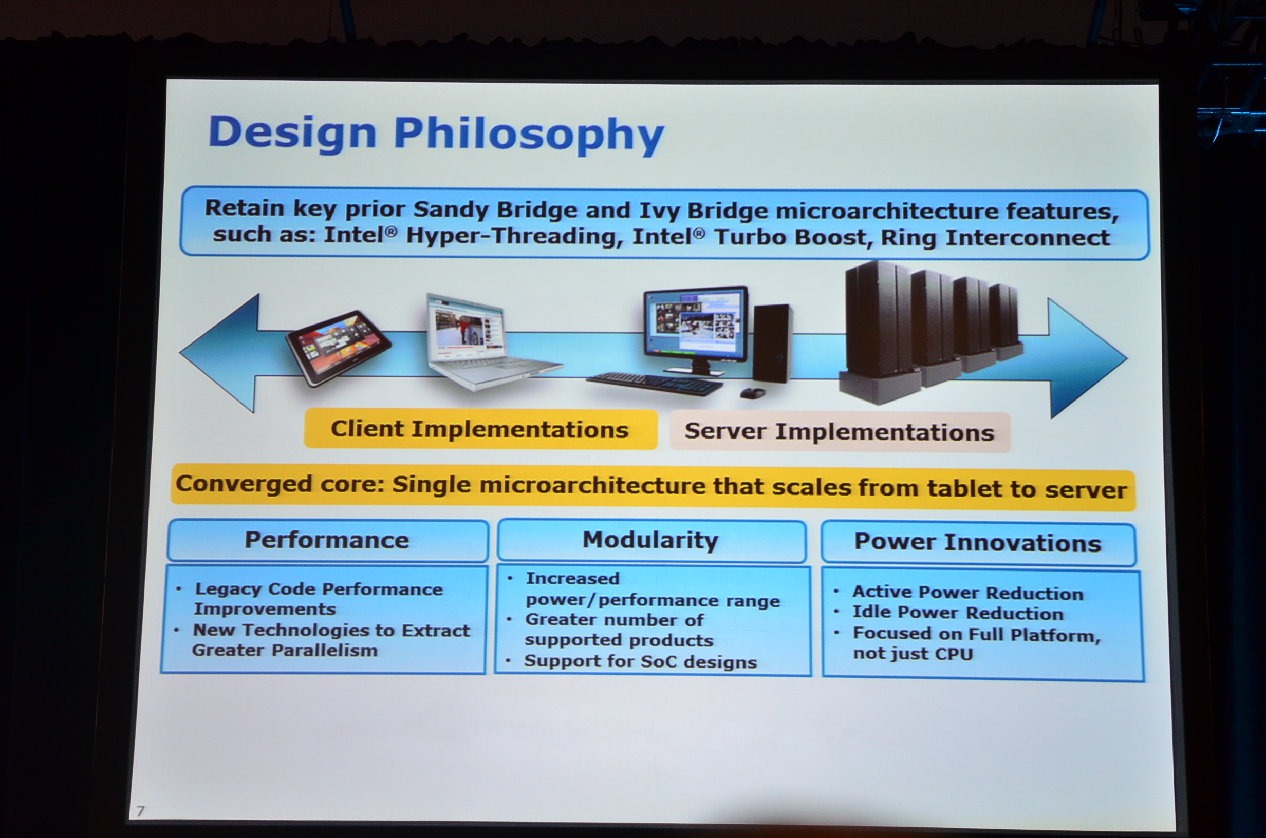
01:35PM - Haswell Design Philosophy: retain prior SNB/IVB microarchitecture features, Hyper Threading, Turbo Boost, Ring Interconnect
01:34PM - Span of Haswell family is larger than previous architectures

01:34PM - Haswell is a tock, second 22nm CPU but significant change at the platform and architectural level
01:32PM - We're going to get a high level architecture disclosure as well as some indication of what we'll see in client deployments of Haswell
01:31PM - Ronak Singhal, one of the Haswell architects, is talking now
01:30PM - Seats are filling up, we're waiting for the session to begin


42 Comments
View All Comments
Mr Perfect - Tuesday, September 11, 2012 - link
AMD and ARM come to mind. You don't have to be winning to be competing.ifrit39 - Tuesday, September 11, 2012 - link
Anand,I find this new live blog feature interesting to say the least, but I don't think it fits into your site well. Allow me to elaborate.
Just yesterday I listened to your podcast episode 4, and I think you made a great point (that I believe you've said a ouple of times in the past) about the "cable tv-fication" of tech sites. I find it a little bit surprising that you're doing this live blog simply because you seemed passionate about this idea. Your point was essentially that so many tech websites are becoming more and more about publishing the latest rumors and snippets of information that stream out from various "sources" that get repeated over and over on other sites with no real substance.
I think that this live blog thing is headed in that exact direction: constant snippets of interesting new information, but no analysis and nothing of substance. You're doing your readers a disservice by delivering intel's keynotes to us with one-liners. I have no clue how the haswell being capable of 2x FMA ops per cycle per core will affect me as a user. I'd personally much prefer you post a short pipeline post, as you have in the past about the news summerized on the day of the event, then have a thorough analysis of the presentation be posted later on.
Despite this, I still want to thank you for everything you do for your readers! I still think AT has the highest standards of any tech site and that's why I keep coming back!
cantcurecancer - Tuesday, September 11, 2012 - link
This is the bread and butter of anandtech though...The sensationalist tech sites didn't even cover this story because it's beyond the scope of those readers (and writers). But you know what, when the next line of tablets and notebooks and MBAs come out, they are going to reference this every single one of these articles like they always do. I see your point, we don't necessarily need a liveblog on something like this, but if Anandtech is able to get the information out faster, why not?Kevin G - Tuesday, September 11, 2012 - link
In fairness, this live blog is coming from a real source: Intel themselves and fits square into the news category and not rumor/speculation.As for 2x FMA, right now only a small benefit as software would have to be recompiled as it uses some new instructions. Basically it allows for two sets of multiply then add functions to be carried out in parallel. The hardware does allow for things like two independent multiplies or two independent adds to be carried out in parallel now. Previously Sandybridge could perform an independent multiply and an independent add. There will be a bit of a benefit for unmodified code but difficult to quantify as optimized code for Sandybridge would avoid that situation.
ifrit39 - Tuesday, September 11, 2012 - link
Thanks for clarifying a bit on the fused-multiply-add thing. I understood at a basic level what the function is for but I was merely using it as an example rather than actually asking what it meant. It was to help illustrate. My point is that we need analysis of what was said at IDF, not one-liner regurgitation.And I get that this is Intel we're talking about. I didn't mean to say that the information isn't reputable, just that its spewed back out at us without any effort on the part of AT.
I think most readers would rather wait a day or so to get the same information in a well organized presentable manner.
Kevin G - Wednesday, September 12, 2012 - link
A correction. It appears that Haswell cannot perform two independent floating point adds simultaneously. It can however perform two independent multiplies as well as two independent FMA.The inability to perform two independent adds is rather puzzling. It wouldn't surprise me if this is one of the minor changes made when they migrate to 14 nm.
name99 - Tuesday, September 11, 2012 - link
2x FMA (and AVX/AVX2) are for high performance floating point. Think matrix multiplication (and everything that ultimately reduces to matrix multiplication, from eigenvalue problems to PDEs).If you don't know how you need it, then you probably don't need it. That's OK --- enjoy the rest of the chip. No-one will use aggressively every feature that is on it.
1008anan - Tuesday, September 11, 2012 - link
ifrit39,We strongly disagree. There was a lot of substance in what Anand was able to summarize. A lot of new substantive news that I didn't know before.
"2* FMA ops per cycle per core is huge. It, combined with other information means that Haswell will be more than two times as fast as Ivy Bridge for a specific watt TDP.
dishayu - Wednesday, September 12, 2012 - link
you DO realize that he's posting this directly from IDF hall, right?You want him to post realtime analysis? Anand has always posted in depth analysis articles after IDF (He did it for Sandy and Ivy as well), but you need to have some patience for that, perhaps? It's rather unrealistic to expect him to do analysis articles on the fly while attending the conference TBH.
JKflipflop98 - Wednesday, September 12, 2012 - link
I really like the liveblog thing. Pretty sure there will be a "real" article with all the info summed up later as is tradition. Like everyone else is saying, if it helps the man get the info out faster, then I'm good with it too.