Preparing for the iPhone Next: Rumors Analyzed
by Brian Klug & Anand Lal Shimpi on August 27, 2012 9:40 PM EST- Posted in
- Smartphones
- Apple
- Mobile
- iPhone
The SoC: 32nm A5R2?
So much of any new iPad/iPhone release is tied to the SoC. Apple remains one of the only handset designers that aggressively specs its own SoC rather than picking up an off the shelf part. As of late, Apple has used its control over its own SoC architecture to better match its chip architectures to the needs of its high resolution displays. Apple continues to produce its custom-designed SoCs at Samsung, although it's likely that Apple will consider other foundries at the 20nm node.
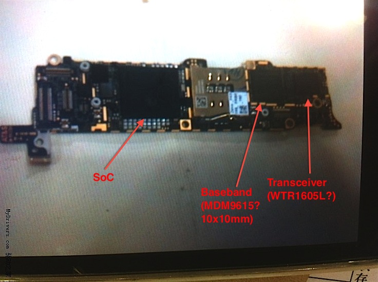

Rumored upcoming PCB, annotations ours
Most early looks at the next iPhone's internals show no silkscreened part numbers on the SoC. We've already seen blurry photos of the suspected upcoming PCB leak, though they're far too low quality to make out any chip markings. Given Apple's history, it's likely we'll see a 32nm LP (HK+MG) variant of the A5 SoC used in the iPhone 4S - perhaps at higher clocks. The move to a smaller process node should bring about a tangible increase in battery life. Depending on the workload, the iPhone 4S could burn more power than the iPhone 4 thanks to its beefy CPU + GPU combination. The move to 32nm could easily offset this penalty.
We've seen Apple experiment with Samsung's 32nm LP process in the past. Both the current generation Apple TV and the iPad 2,4 use a 32nm A5. In the case of the iPad 2,4, we saw a huge increase in battery life as a result of the move to 32nm. Some of the gains in battery life in the iPhone are likely to be offset by higher CPU/GPU clocks, but this is still the most likely approach for Apple this generation.

Original A5 (45nm, S5L8940, left), A5R2 (32nm, S5L8942, right)
As we mentioned back during our review of the iPad 2,4, it makes sense to test a new/unfamiliar process on a low volume part. By shipping 32nm A5 SoCs into some iPad 2s and the Apple TV (a hobby product), Apple could ride the 32nm yield curve up without adversely impacting shipments of its key money makers. With Samsung's 32nm LP process likely seeing much better yields now, it's time to deploy it in the next iPhone. Given much of the competition has moved to TSMC's 28nm process, Apple must remain competitive on the process node front as well. Shipping a 45nm SoC at the end of 2012 simply doesn't make sense. Although the current legal battles with Samsung could impact the relationship on the foundry side, simply switching to Global Foundries or TSMC is easier said than done. I would expect Apple to go through the same careful transition between Samsung and any other foundry as it did when it introduced the first 32nm A5s into the mix. The current expectations here are that we'll see Apple look at TSMC at the 20nm node.
With process node pretty much guaranteed, there's the question of CPU and GPU architectures.
Since the release of the original iPad, Apple has used the spring to introduce new SoC architectures in the iPad and later waterfall them down to the iPhone in the summer/fall. The A5X in the 3rd generation iPad however is still built on Samsung's 45nm LP process and is huge as a result of integrating four PowerVR SGX543 cores and implementing a 4 x 32-bit memory interface. The A5X needed the GPU power and memory bandwidth to drive the new iPad's retina display, but that power would be largely lost on the next iPhone.
The new iPhone is expected to have a 640 x 1136 resolution, thanks to its taller 4-inch display, but that's only 18% more pixels than the current iPhone 4S. A doubling of memory bandwidth and GPU compute horsepower would seem a bit excessive for current workloads. A ~20% increase in GPU clock speed, and faster DRAM would be enough to maintain current levels of performance on the higher resolution display.
Apple decoupled major cellular architecture and CPU architecture shifts in the past (e.g. iPhone 3G/3GS transition), which lends credibility to the idea of a move to A15 next year with the 4th gen iPad and sticking with the dual-core A9 design for the next iPhone. There's also the fact that TI is expected to be one of the first to bring an ARM Cortex A15 based SoC to market, and even it hasn't demonstrated an OMAP 5 running at shipping CPU clocks yet. I don't doubt that it's possible to ship an A15 based SoC before the end of the year, but based on the demos we've seen thus far, it seems highly unlikely to see one shipping in Q3. Apple doesn't like to be overly risky on the component front. There's nothing worse than a poorly yielding or otherwise problematic chip holding up shipments of one of your biggest revenue generators.


131 Comments
View All Comments
jlbenton - Tuesday, September 11, 2012 - link
Reading the section on NFC, I see a few misleading facts presented. An NFC antenna can work when place on a piece of metal. It basically needs a ferrous film attached to the flat flex circuit to reflect the magnetic waves to the antenna and not to be absorbed by the metal shield.I have designed a few NFC antennas and found you can get them much smaller than you might think.
Bluetooth LE would never be used for mobile payments as it is not secure. It's transmit range is much larger than NFC. Someone next to you could easily intercept the signal just standing next to you in the grocery store. QR codes take too long to take a photo of, a step backwards compared to a swipe of a card. If Apple is serious about mobile payments, which I believe they should be due to the potential for profits, then NFC is the only answer.