ASRock Z77 Extreme6 Review: Legacy Bites Back
by Ian Cutress on July 13, 2012 2:00 PM EST- Posted in
- Motherboards
- ASRock
- Z77
ASRock are not afraid of the legacy connections. Not merely content on having both a floppy drive header and an IDE connector on the Fatal1ty Z77 Professional, they have also put a floppy header on the Z77 Extreme6. There is reason for this, given that industrial equipment can cost $millions and a shiny new PC to process the data costs a lot less, even if they can only communicate via Floppy. Today we are looking at the performance and package that comes with the Z77 Extreme6, and see if it holds up with its price tag against the vast array of Z77 motherboards currently on the market.
ASRock Z77 Extreme6 Overview
Performance is an odd test on a motherboard for the most part. Every major facet of the motherboard is often in the control of something else - the CPU takes care of computation, the RAM looks after local data management, the chipset for IO, and audio for audio. The motherboard is merely the collection of controllers collated with design, with a vendor specific flair of aesthetics and software on top. So why test the performance?
More often than not, in each of the circumstances listed above, the motherboard comes in as the second most important feature. The routing between two components will determine the latency, or the decision to use one port per controller rather than two may influence throughput. These differences do not show up significantly during testing (CPU tests, for example) unless the motherboard becomes the limiting factor in some regard. This is why we try to test with the best CPU, the best memory, and so on. However, areas such as the DPC Latency (how the CPU and chipset deal with requests) are governed by the BIOS, something that the motherboard directly influences.
Thus, if a motherboard happened to perform near the bottom in the majority of the tests is quite alarming - somehow, the board has a flaw at some level. What if the difference between the board and the second from bottom board was very slight every time, coming in at less than 1%? How would we analyze such a product? Would it be bad?
Unfortunately, this is where the Z77 Extreme6 fits in many of our tests. It lacks the MultiCore Enhancement that both ASUS and Gigabyte apply to their boards for extra MHz at full loading, as well as long-term stability with my standard G.Skill DDR3-2400 testing kit.
This is not a concern if you run an overclock though, as the Z77 Extreme6 board overclocks the CPU quite well, reaching 4.7 GHz on our test chip with 1.175 volts in the BIOS and only 82ºC during OCCT.
Software wise, ASRock has paired the Extreme6 with their normal feature set plus a couple of bonuses for Z77 - namely their Online Management Guard facility and 'Dehumidifier Function'. These two lack significant substance by being only BIOS based utilities though - ideally, a software implementation would be preferred.
For the price, we get ASRock's great little USB 3.0 bracket in the box, as well as a complete set of video outputs on the IO. As a sneaky little addition as well, users can put in three AMD GPUs for 3-way CFX, if you do not mind the third card limited to x4 PCIe 2.0 coming from the chipset (analyzed later in the review). This does away with the need for a PLX PXE 8747 chip on board, which would have increased the price by another $30 or so.
The ASRock Z77 Extreme6 is a capable motherboard for most usage scenarios. Just add some nice DDR3-2133 memory and apply a CPU overclock. However, it lacks some substance and a spark over other major motherboard manufacturers.
Visual Inspection
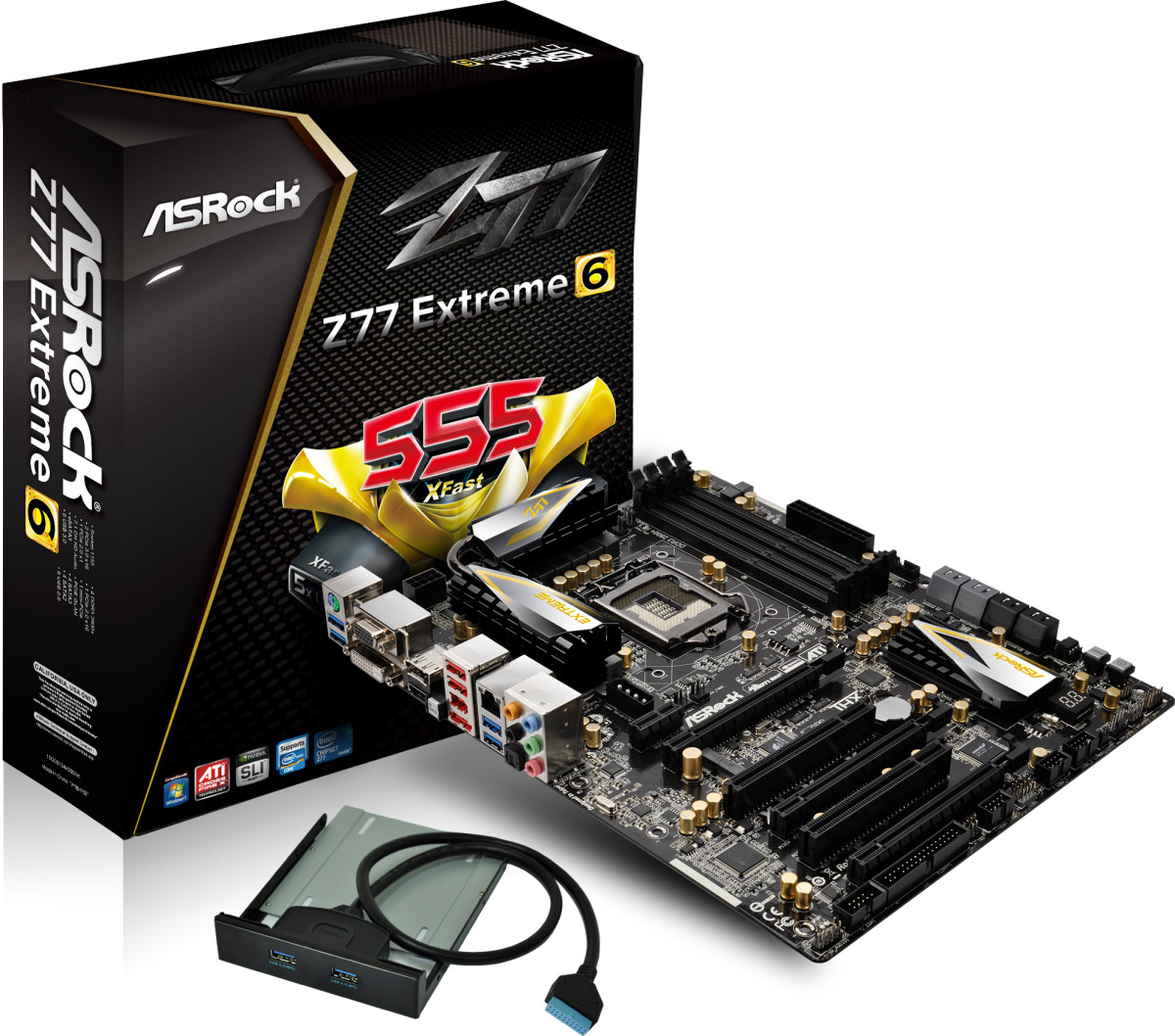
With the Z77 Extreme6, compared to the Z77 Extreme4, there are a significant number of changes, both visual and in terms of features. For a start, the heatsink design is more pronounced, using something similar to their X79 range in terms of black and gold ridged and edged surfaces.
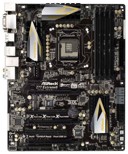
Onboard is also an mSATA port, right in the middle between the first PCIe slot and the PCI slot. Above the PCIe slots is a 4-pin molex power connector to provide extra power to the PCIe slots, although I am kind of getting tired of seeing it put in this location. If anything, it should be at the bottom end or beside the 24-pin power connector, as having it above the PCIe slots just means that there will be cables all over the place.
One other less obvious change to the Z77 Extreme4 is that there is a Floppy drive header on board. Yes, you heard me right – floppy drive! It seems odd now to include this legacy connection. It still has a place in industrial concepts (where a machine uses floppy drives and costs 1000x more than the PC processing its data), but not particularly on a higher end product which may be geared towards gaming and overclocking. As ASRock seem to be the only manufacturer pursuing this path on their consumer line, then it creates a niche just for them.
In terms of fan headers on board, we have one three-pin beside the 8-pin 12V power connector, two CPU headers (one 4-pin, one 3-pin) just to the right of the top heatsink, two chassis three-pin headers beside the molex connector, and another 4-pin chassis header on the bottom of the board. On the right hand side, the USB 3.0 connector has been placed beneath the 24-pin ATX power connector, followed by the SATA ports. Like the Extreme4, we have the PCH SATA ports (two SATA 6 Gbps and four SATA 3 Gbps) and two extra SATA 6 Gbps from an ASMedia ASM1061 controller.
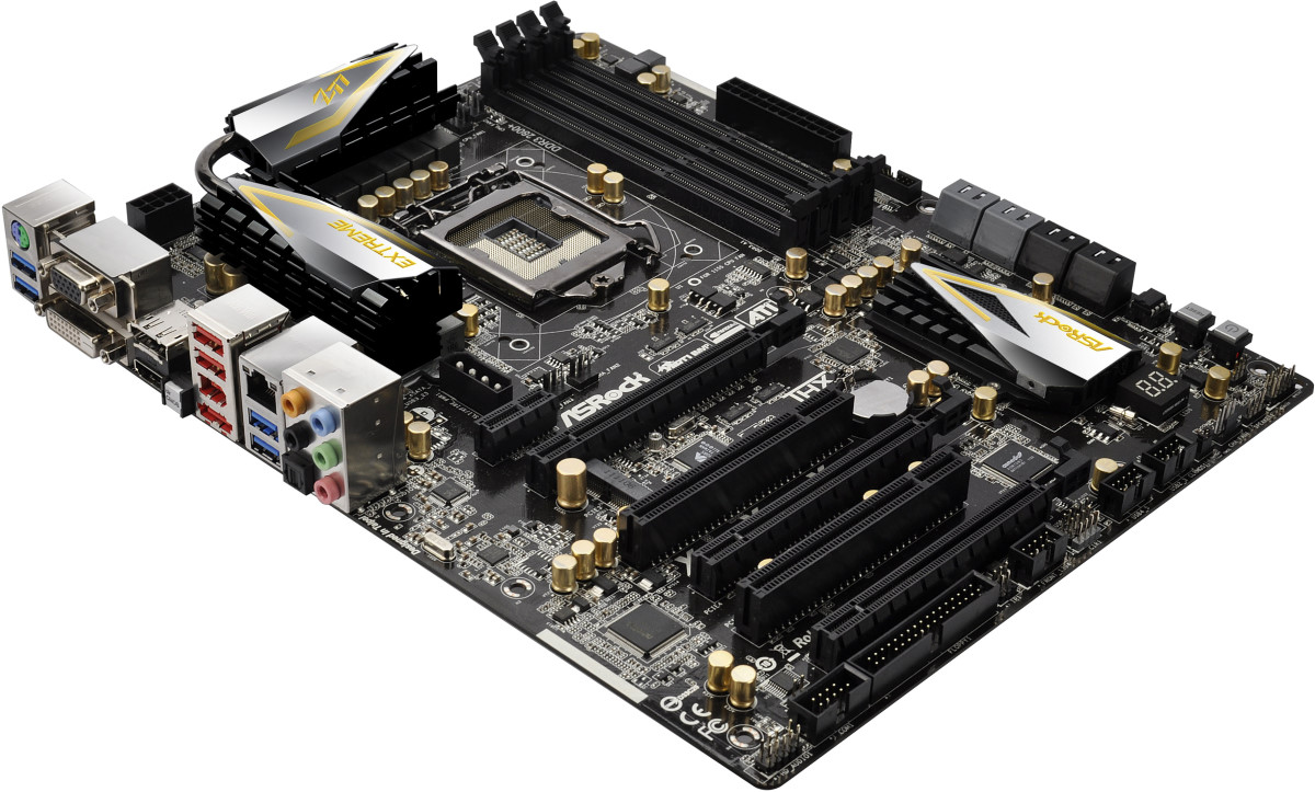
Around the larger chipset heatsink, we have power/reset buttons and a two digit debug display, both of which I personally like to see as a reviewer (makes my job a bit easier) but also helps overclockers. On the south side of the board, apart from that floppy connector I mentioned, we have a COM port, front panel audio, and an array of USB 2.0 headers.
PCIe layout is similar to the Z77 Extreme4, with a PCIe x1, PCIe 3.0 x16/x8, an mSATA connector, PCI, PCIe 3.0 x8, PCI, and a PCI 2.0 x4. This allows a user to use a dual GPU setup, and still have access to a PCIe x1 and x4.
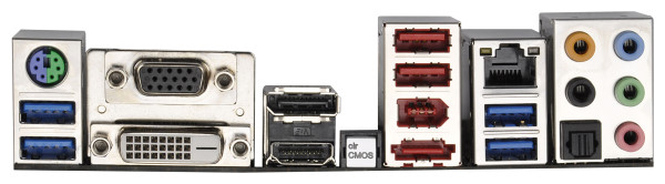
Aside from the bowed picture from ASRock, we have something similar to the Extreme4 for the IO back panel, though this time with a DisplayPort output. From left to right, we have a combination PS/2 port, two USB 3.0 ports (blue), a D-Sub port, DVI-D, DisplayPort, HDMI, a ClearCMOS button, two USB 2.0 (red), an IEEE1394 port, eSATA, gigabit Ethernet, two more USB 3.0 (blue), and audio outputs including an optical SPDIF.
Board Features
| ASRock Z77 Extreme6 | |
| Price | Link |
| Size | ATX |
| CPU Interface | LGA-1155 |
| Chipset | Intel Z77 |
| Memory Slots |
Four DDR3 DIMM slots supporting up to 32 GB Up to Dual Channel, 1066-2800 MHz |
| Video Outputs | DisplayPort, HDMI 1.4a, DVI-D, D-Sub |
| Onboard LAN | Broadcom BCM57781 |
| Onboard Audio | Realtek ALC898 |
| Expansion Slots |
2 x PCIe x16 Gen3 (x16, x8/8) 1 x PCIe x16 Gen2 (x4) 1 x PCIe x1 Gen2 2 x PCI 1 x mini PCIe |
| Onboard SATA/RAID |
2 x SATA 6 Gbps (PCH), Support for RAID 0, 1, 5, 10 2 x SATA 6 Gbps (ASMedia ASM1061) 4 x SATA 3 Gbps (PCH), Support for RAID 0, 1, 5, 10 |
| USB |
Two USB 3.0 at rear (PCH) Two USB 3.0 at rear (Etron EJ168A) One USB 3.0 header (PCH) |
| Onboard |
4 x SATA 6 Gbps 4 x SATA 3 Gbps 1 x Floppy Connector 1 x IR Header 1 x CIR Header 1 x COM Header 1 x SPDIF Header 1 x 4-pin Molex power connector Power/Reset Buttons Two Digit Debug LED 6 x Fan Headers Front panel audio connector 3 x USB 2.0 headers (support 6 USB 2.0 ports) 1 x USB 3.0 header (supports 2 USB 3.0 ports) |
| Power Connectors |
1 x 24-pin ATX connector 1 x 8-pin 12V connector 1 x 4-pin Molex for PCIe |
| Fan Headers |
2 x CPU Fan Header (one 4-pin, one 3-pin) 3 x CHA Fan Headers (one 4-pin, two 3-pin) 1 x SYS Fan Header (one 3-pin) |
| IO Panel |
1 x Combo PS/2 Port 1 x DisplayPort 1 x HDMI 1.4a 1 x DVI-D 1 x D-Sub 1 x Optical SPDIF 2 x USB 2.0 4 x USB 3.0 1 x IEEE1394 1 x Gigabit Ethernet 1 x Clear CMOS Audio Outputs |
| Warranty Period | 3 years from date of purchase |
| Product Page | Link |
Nothing immediately jumps out from the board features list aside from the differences to the Z77 Extreme4. This is a quite good package for an MSRP of $175.


35 Comments
View All Comments
IanCutress - Monday, July 16, 2012 - link
You would be surprised at how regular these timings are. For the 10.81 seconds, I got that on my manual stop watch three times in a row. To do as you suggest would be a heavily distorted effort vs. reward, especially for motherboard reviews. Interesting exercise though, not sure if it would be possible. Not that I'd know how either :)Ian
Demon-Xanth - Monday, July 16, 2012 - link
These days I think the truly best way to support legacy is by add-in cards, and am kind of surprised nobody has come up with a 486 era style I/O card that has serial, parallel, floppy, and IDE on a single card. Just use an older PCI southbridge on a PCIe bridge and you can add some USB to the mix as well.stedaniels - Tuesday, July 24, 2012 - link
Hi,I've been doing some research on this board and notice that you kept referring to the mini PCIe slot as an mSATA slot. While these are physically the same slot size, they are electrically different. Both the specs at the end of the first page, and on the ASRock website state that this is a mini PCIe slot and there is no mention of it being an mSATA slot on any of the official documentation.
Was this a mistake during the review, or are the ASRock specs wrong?
Cheers,
Steve
Mike89 - Friday, January 11, 2013 - link
The settings I've tried give voltage readings way different than this review. For example the review stated the automatic overclock of 4.4 gigs at 1.096 volts at load but when I used that same setting I got a voltage of 1.22 at load. That's quite a bit of difference. Other oc settings I tried that were in the review were also a lot different than the view being they were all higher voltages than the review stated. Can't quite figure out why that is.flexy - Tuesday, April 24, 2018 - link
This is an older article, but since I am OC testing an older Haswell system right now.These numbers seem STRANGE if not outright fantasy to me. What is that "ES" version of the i5 anyway, I can't get any information on this.
The article states they run at 44x multi stable w/ 1.096V in bios, in OCCT/Povray, and stable at 1.100 in bios (1.096 measured under load) at 45x, in OCCT and Povray. Of course, LLC = 1.
What "wonder chip" is that supposed to be that runs stable at a 45x multi in OCCT at 1.096 volts? I am having a very hard time taking these numbers seriously, unless you used some extremely carefully select CPUs with amazingly low power requirements and temps for your testing. (At these voltages I can't even get into the OS, even with LLC1, not to mention OCCT.)