The AMD Trinity Review (A10-4600M): A New Hope
by Jarred Walton on May 15, 2012 12:00 AM ESTImproved Turbo
Trinity features a much improved version of AMD's Turbo Core technology compared to Llano. First and foremost, both CPU and GPU turbo are now supported. In Llano only the CPU cores could turbo up if there was additional TDP headroom available, while the GPU cores ran no higher than their max specified frequency. In Trinity, if the CPU cores aren't using all of their allocated TDP but the GPU is under heavy load, it can exceed its typical max frequency to capitalize on the available TDP. The same obviously works in reverse.
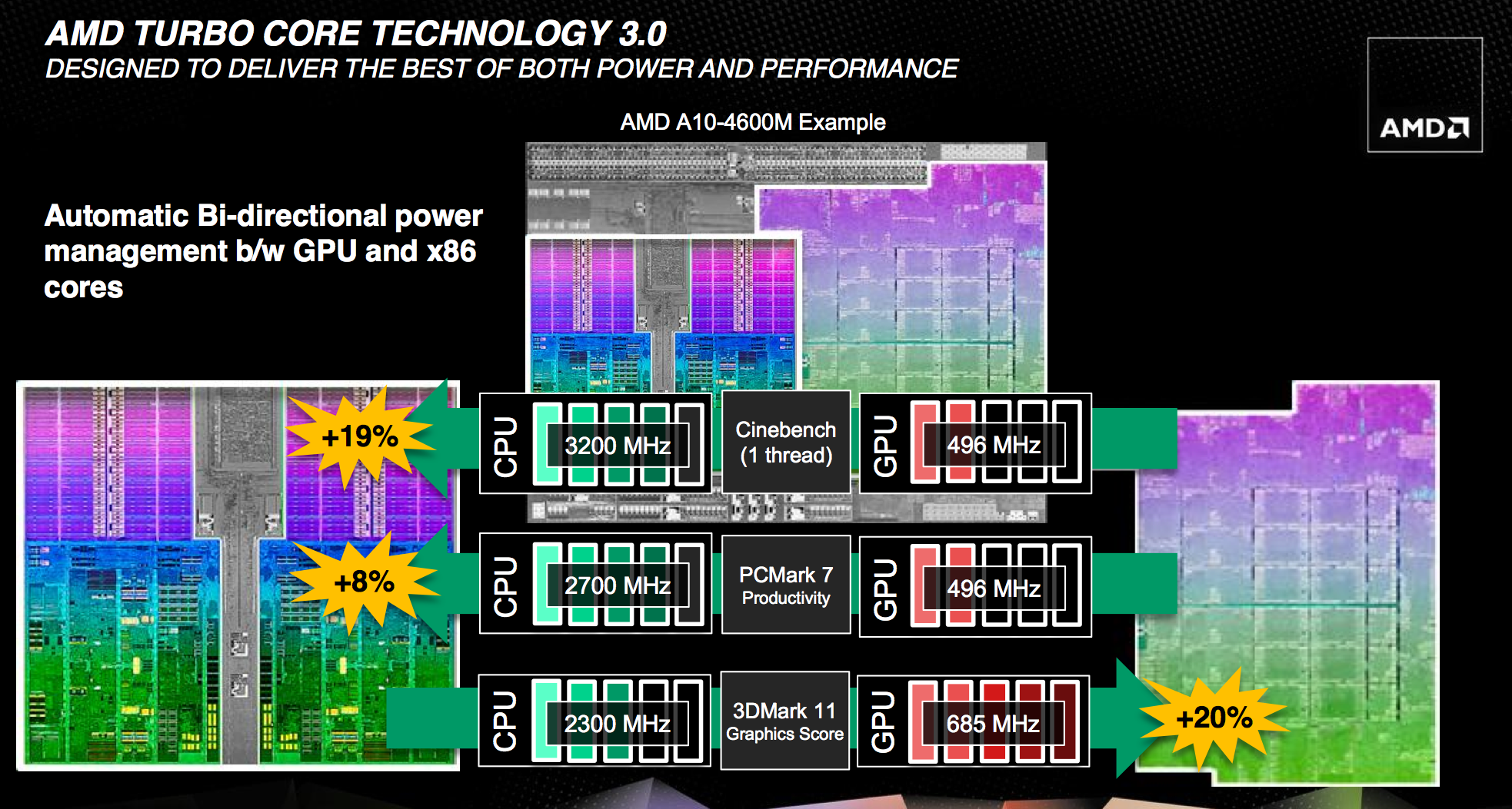
Under the hood, the microcontroller that monitors all power consumption within the APU is much more capable. In Llano, the Turbo Core microcontroller looked at activity on the CPU/GPU and performed a static allocation of power based on this data. In Trinity, AMD implemented a physics based thermal calculation model using fast transforms. The model takes power and translates it into a dynamic temperature calculation. Power is still estimated based on workload, which AMD claims has less than a 1% error rate, but the new model gets accurate temperatures from those estimations. The thermal model delivers accuracy at or below 2C, in real time. Having more accurate thermal data allows the turbo microcontroller to respond quicker, which should allow for frequencies to scale up and down more effectively.
At the end of the day this should improve performance, although it's difficult to compare directly to Llano since so much has changed between the two APUs. Just as with Llano, AMD specifies nominal and max turbo frequencies for the Trinity CPU/GPU.
A Beefy Set of Interconnects
The holy grail for AMD (and Intel for that matter) is a single piece of silicon with CPU and GPU style cores that coexist harmoniously, each doing what they do best. We're not quite there yet, but in pursuit of that goal it's important to have tons of bandwidth available on chip.
Trinity still features two 64-bit DDR3 memory controllers with support for up to DDR3-1866 speeds. The controllers add support for 1.25V memory. Notebook bound Trinities (Socket FS1r2 and Socket FP2) support up to 32GB of memory, while the desktop variants (Socket FM2) can handle up to 64GB.
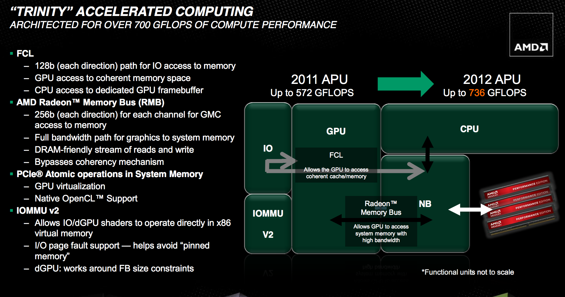
Hyper Transport is gone as an external interconnect, leaving only PCIe for off-chip IO. The Fusion Control Link is a 128-bit (each direction) interface giving off-chip IO devices access to system memory. Trinity also features a 256-bit (in each direction, per memory channel) Radeon Memory Bus (RMB) direct access to the DRAM controllers. The excessive width of this bus likely implies that it's also used for CPU/GPU communication as well.
IOMMU v2 is also supported by Trinity, giving supported discrete GPUs (e.g. Tahiti) access to the CPU's virtual memory. In Llano, you used to take data from disk, copy it to memory, then copy it from the CPU's address space to pinned memory that's accessible by the GPU, then the GPU gets it and brings it into its frame buffer. By having access to the CPU's virtual address space now the data goes from disk, to memory, then directly to the GPU's memory—you skip that intermediate mem to mem copy. Eventually we'll get to the point where there's truly one unified address space, but steps like these are what will get us there.
The Trinity GPU
Trinity's GPU is probably the most well understood part of the chip, seeing as how its basically a cut down Cayman from AMD's Northern Islands family. The VLIW4 design features 6 SIMD engines, each with 16 VLIW4 arrays, for a total of up to 384 cores. The A10 SKUs get 384 cores while the lower end A8 and A6 parts get 256 and 192, respectively. FP64 is supported but at 1/16 the FP32 rate.
As AMD never released any low-end Northern Islands VLIW4 parts, Trinity's GPU is a bit unique. It technically has fewer cores than Llano's GPU, but as we saw with AMD's transition from VLIW5 to VLIW4, the loss didn't really impact performance but rather drove up efficiency. Remember that most of the time that 5th unit in AMD's VLIW5 architectures went unused.
The design features 24 texture units and 8 ROPs, in line with what you'd expect from what's effectively 1/4 of a Cayman/Radeon HD 6970. Clock speeds are obviously lower than a full blown Cayman, but not by a ton. Trinity's GPU runs at a normal maximum of 497MHz and can turbo up as high as 686MHz.
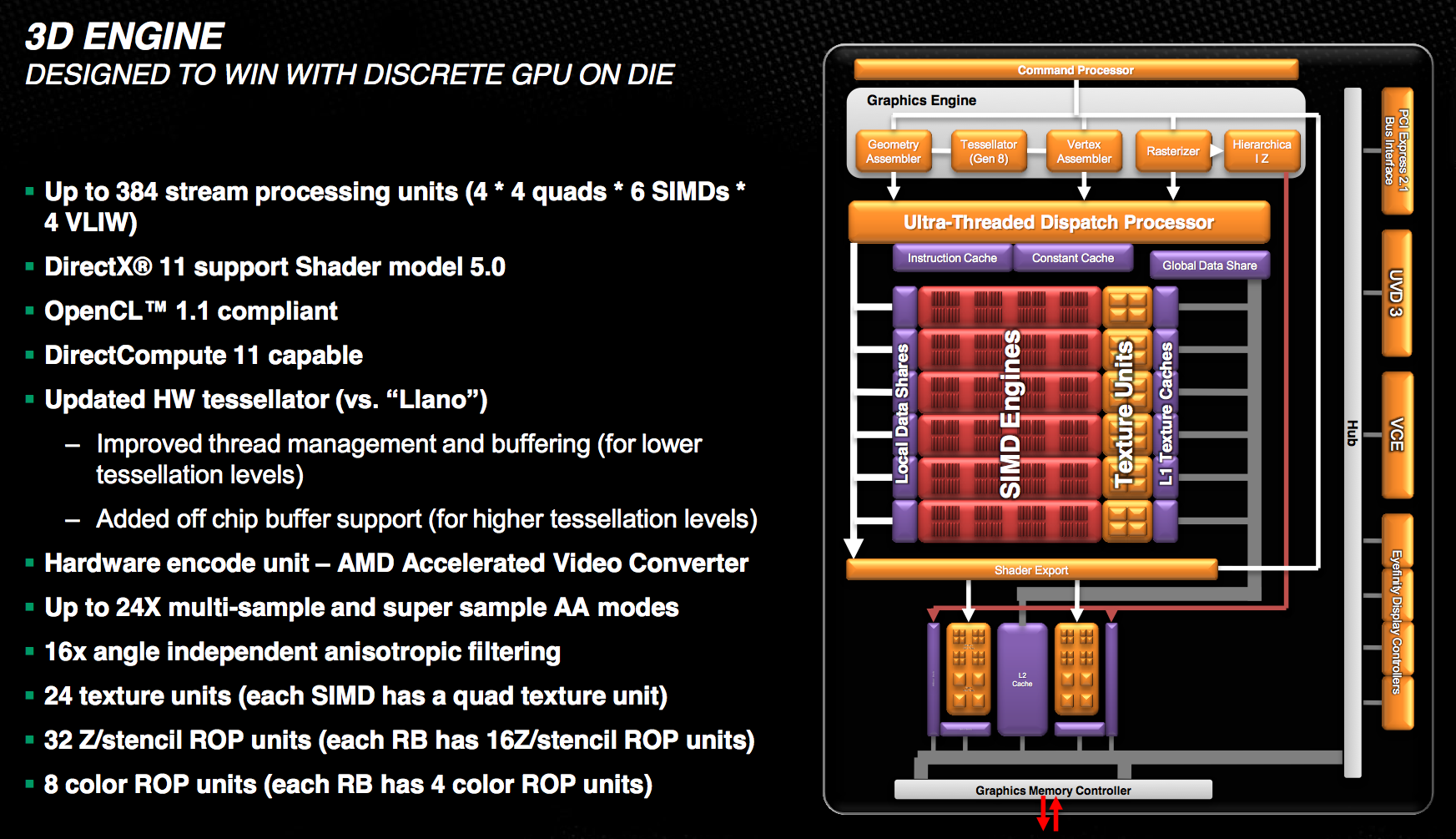
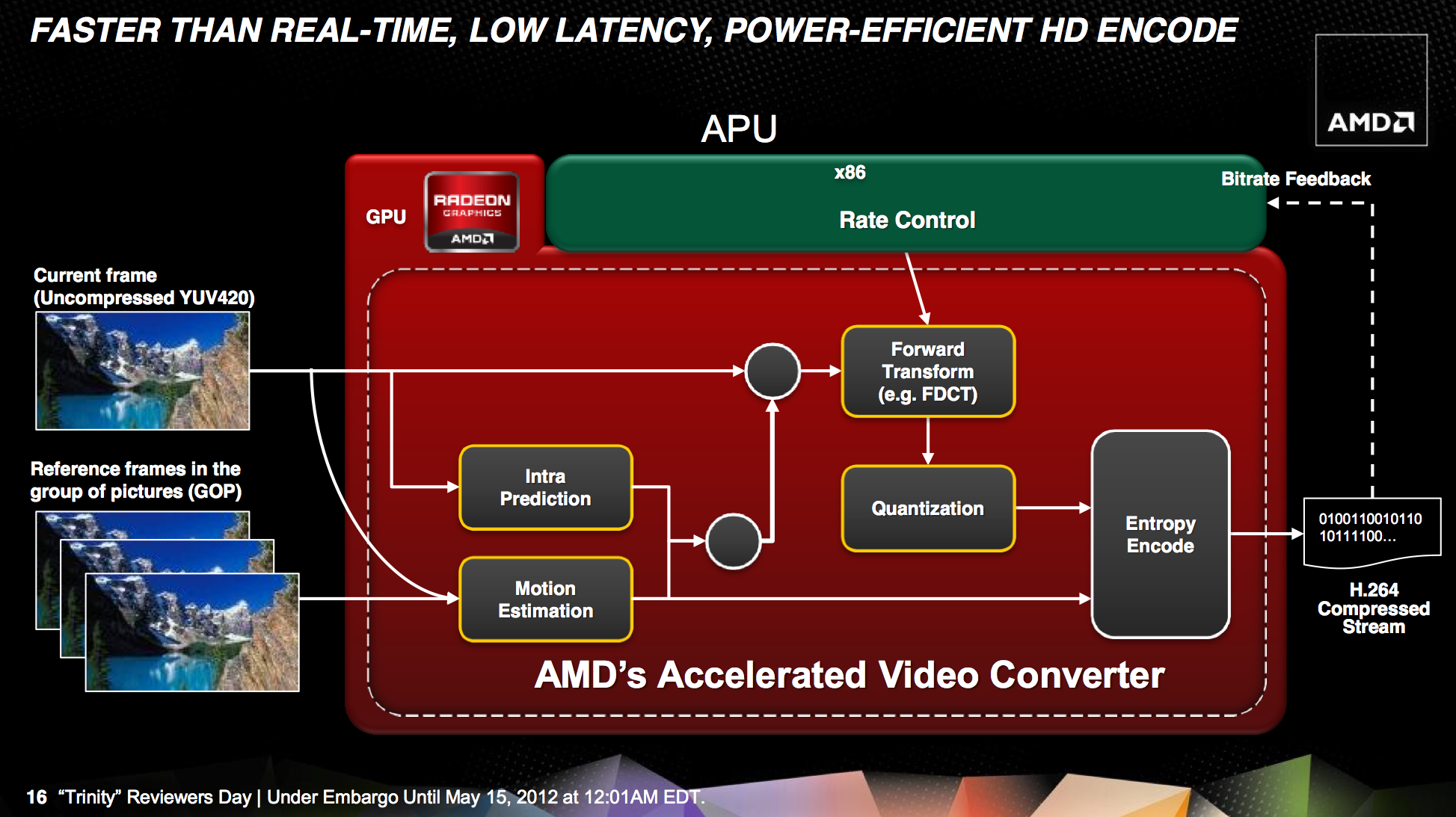
Trinity includes AMD's HD Media Accelerator, which includes accelerated video decode (UVD3) and encode components (VCE). Trinity borrows Graphics Core Next's Video Codec Engine (VCE) and is actually functional in the hardware/software we have here today. Don't get too excited though; the VCE enabled software we have today won't take advantage of the identical hardware in discrete GCN GPUs. AMD tells us this is purely a matter of having the resources to prioritize Trinity first, and that discrete GPU VCE support is coming.


271 Comments
View All Comments
raghu78 - Tuesday, May 15, 2012 - link
AMD needs to do much better with their CPU performance otherwise its looking pretty bad from here.Intel Haswell is going to improve the graphics performance much more significantly. With some rumours of stacked DRAM making it to haswell it looks pretty grim from here. And we don't know the magnitude of CPU performance improvements in Haswell ? AMD runs the risk of becoming completely outclassed in both departments. AMD needs to have a much better processor with Steamroller or its pretty much game over. AMD's efforts with HSA and OpenCL are going to be very crucial in differentiating their products. Also when adding more GPU performance AMD needs to address the bandwidth issue with some kind of stacked DRAM solution. AMD Kaveri with 512 GCN cores is going to be more bottlenecked than Trinity if their CPU part isn't much more powerful and their bandwidth issues are not addressed. I am still hoping AMD does not become irrelevant cause comeptition is crucial for maximum benefit to the industry and the market.
Kjella - Tuesday, May 15, 2012 - link
Well it's hard to tell facts from fiction but some have said Haswell will get 40 EUs as opposed to Ivy Bridge's 16. Hard to say but we know:1. Intel has the TDP headroom if they raise it back up to 95W for the new EUs.
2. Intel has the die room, the Ivy Bridge chips are Intel's smallest in a long time.
3. Graphics performance is heavily tied to number of shaders.
In other words, if Intel wants to make a much more graphics-heavy chip - it'll be more GPU than CPU at that point - they can, and I don't really see a good reason why not. Giving AMD and nVidia's low end a good punch must be good for Intel.
mschira - Tuesday, May 15, 2012 - link
Hellooouuu?Do I see this right? The new AMD part offers better battery life with a 32 nm part than Intel with a spanking new 22nm part?
And CPU performance is good (though not great...)?
AND they will offer a 25W part that will probably offer very decent performance but even better battery life?
And you call this NOT earth shattering?
I don't understand you guys.
I just don't.
M.
JarredWalton - Tuesday, May 15, 2012 - link
Intel's own 32nm part beats their 22nm part, so no, I'm not surprised that a mature 32nm CPU from AMD is doing the same.Spunjji - Tuesday, May 15, 2012 - link
...that makes sense if you're ignoring GPU performance. If you're not, this does indeed look pretty fantastic and is a frankly amazing turnaround from the folks that only very recently brought us Faildozer.I'm not going to chime in with the "INTEL BIAS" blowhards about, but I do agree with mschira that this is a hell of a feat of engineering.
texasti89 - Tuesday, May 15, 2012 - link
"Intel's own 32nm part beats their 22nm part", how so?CPU improvement (clk-per-clk) = 5-10%
GPU improvement around 200%
Power efficiency (for similar models) = 20-30% power reduction.
JarredWalton - Tuesday, May 15, 2012 - link
Just in case you're wondering, I might have access to some other hardware that confirms my feeling that IVB is using more power under light loads than SNB. Note that we're talking notebooks here, not desktops, and we're looking at battery life, not system power draw. So I was specifically referring to the fact that several SNB laptops were able to surpass the initial IVB laptop on normalized battery life -- nothing more.vegemeister - Tuesday, May 15, 2012 - link
Speaking of which, why aren't you directly measuring system power draw? Much less room for error than relying on manufacturer battery specifications, and you don't have to wait for the battery to run down.JarredWalton - Wednesday, May 16, 2012 - link
Because measuring system power draw introduces other variables, like AC adapter efficiency for one. Whether we're on batter power or plugged in, the reality is that BIOS/firmware can have an impact on these areas. While it may only be a couple watts, for a laptop that's significant -- most laptops now idle at less than 9W for example (unless they have an always on discrete GPU).vegemeister - Wednesday, May 16, 2012 - link
You could measure on the DC side. And if you want to minimize non-CPU-related variation, it would be best to do these tests with the display turned off. At 100 nits you'll still get variation from the size of the display and the efficiency of the inverter and backlight arrangement.