NVIDIA GeForce GTX 680 Review: Retaking The Performance Crown
by Ryan Smith on March 22, 2012 9:00 AM ESTGPU Boost: Turbo For GPUs
Now that we’ve had a chance to take a look at the Kepler architecture, let’s jump into features. We’ll start with the feature that’s going to have the biggest impact on performance: GPU Boost.
Much like we’ve seen with CPUs in previous years, GPUs are reaching a point where performance is being limited by overall power consumption. Until the last couple of years GPU power consumption has been allowed to slowly drift up with each generation, allowing for performance to scale to an incredible degree. However for many of the same reasons NVIDIA has been focusing on efficiency in general, GPUs are being pressured to do more without consuming more.
The problem of course is compounded by the fact that there are a wide range of possible workloads for a GPU, much like there is for a CPU. With the need to design video cards around specific TDPs for both power supply and heat dissipation reasons, the goal becomes one of maximizing your performance inside of your assigned TDP.
The answer to that problem in the CPU space is turbo boosting – that is increasing the clockspeed of one or more CPU cores so long as the chip as a whole remains at or under its TDP. By using turbo, Intel and AMD have been able to both maximize the performance of lightly threaded applications by boosting a handful of cores to high speeds, and at the same time maximize heavily threaded performance by boosting a large number of cores by little to none. For virtually any CPU-bound workload the CPU can put itself into a state where the appropriate execution units are making the most of their TDP allocation.
Of course in the GPU world things aren’t that simple – for starters we don’t have a good analogy for a lightly threaded workload – but the concept is similar. GPUs need to be able to run demanding tasks such as Metro 2033 or even pathological applications like FurMark while staying within their designated TDPs, and at the same time they need to be sure to deliver good performance for compute applications and games that aren’t quite so demanding. Or put another way, tasks that are GPU limited but aren’t maxing out every aspect of the GPU need to be able to get good performance without being held back by the need to keep heavy workloads in check.
In 2010 AMD took a stab that this scenario with PowerTune, which was first introduced on the Radeon HD 6900 series. With PowerTune AMD could set their clockspeeds relatively high, and should any application demand too much of the GPU, PowerTune would throttle down the GPU in order to avoid going over its TDP. In essence with PowerTune the GPU could be clocked too high, and simply throttled down if it tried to draw too much power. This allowed lighter workloads to operate at higher clockspeeds, while keeping power consumption in check for heavy workloads.
With the introduction of Kepler NVIDIA is going to be tackling this problem for their products, and their answer is GPU Boost.
In a nutshell, GPU Boost is turbo for the GPU. With GPU Boost NVIDIA is able to increase the core clock of GTX beyond its 1006MHz base clock, and like turbo on CPUs this is based on the power load, the GPU temperature, and the overall quality of the GPU. Given the right workload the GTX 680 can boost by 100MHz or more, while under a heavy workload the GTX 680 may not move past 1006MHz.
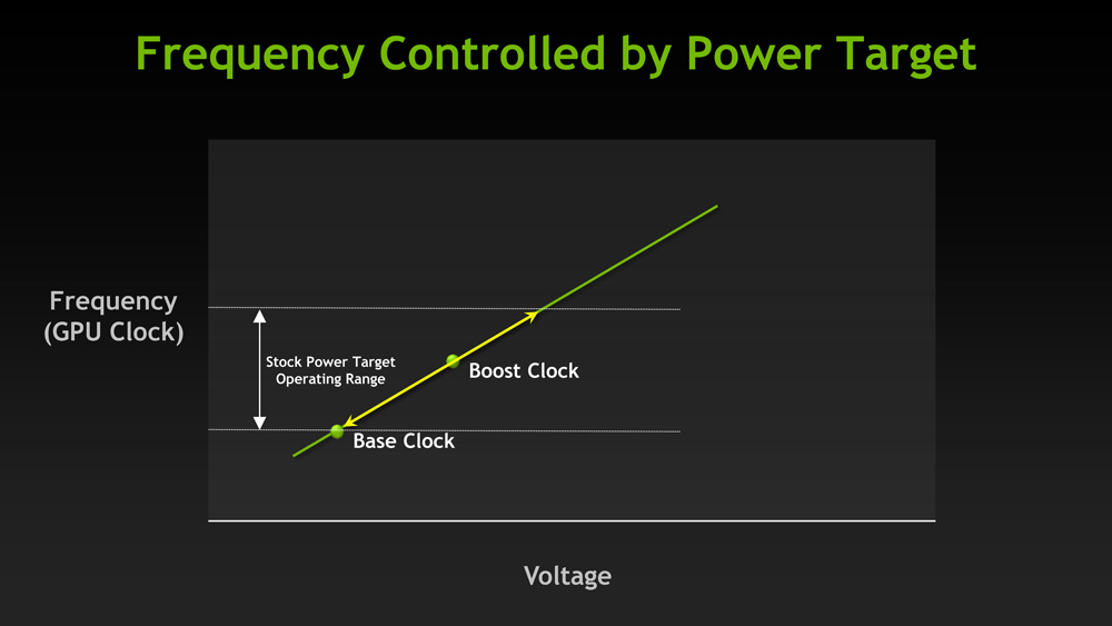
With GPU Boost in play this adds a new wrinkle to performance of course, but ultimately there are 2 numbers to pay attention to. The first number is what NVIDIA calls the base clock: this is another name for the regular core clock, and it represents the minimum full load clock for GTX 680; when operating at its full 3D clocks, the GTX 680 will never drop below this number.
The second number is what NVIDIA calls the boost clock, and this one is far more nebulous, as it relates to the operation of GPU Boost itself. With GPU Boost NVIDIA does not have an explicit top clock; they’re letting chip quality play a significant role in GPU Boost. Because GPU Boost is based around power consumption and temperatures, higher quality GPUs that operate with lower power consumption can boost higher than lower quality GPUs with higher power consumption. In essence the quality of the chip determines its boost limit under normal circumstances.
Accordingly, the boost clock is intended to convey what kind of clockspeeds buyers can expect to see with the average GTX 680. Specifically, the boost clock is based on the average clockspeed of the average GTX 680 that NVIDIA has seen in their labs. This is what NVIDIA had to say about the boost clock in their reviewer’s guide:
The “Boost Clock” is the average clock frequency the GPU will run under load in many typical non-TDP apps that require less GPU power consumption. On average, the typical Boost Clock provided by GPU Boost in GeForce GTX 680 is 1058MHz, an improvement of just over 5%. The Boost Clock is a typical clock level achieved running a typical game in a typical environment
In other words, when the average GTX 680 is boosting it reaches 1058MHz on average.
Ultimately NVIDIA and their customers are going to go through some teething issues on this, and there’s no way around it. Although the idea of variable performance isn’t a new one – we already see this to some degree with CPU turbo – this is the first time we’ve seen something like this in the GPU space, and it’s going to take some time to get used to.
In any case while we can’t relate to you what the average GTX 680 does with GPU Boost, we can tell you about GPU Boost based on what we’ve seen with our review sample.
First and foremost, GPU Boost operates on the concept of steps, analogous to multipliers on a CPU. Our card has 9 steps, each 13MHz apart, ranging from 1006MHz to 1110MHz. And while it’s not clear whether every GTX 680 steps up in 13MHz increments, based on NVIDIA’s boost clock of 1058MHz this would appear to be the case, as that would be 4 steps over the base clock.
At each step our card uses a different voltage, listed in the table below. We should note that we’ve seen different voltages reported for the same step in some cases, so it’s not entirely clear what’s going on. In any case we’re listing the most common voltage we’ve recorded for each step.
| GeForce GTX 680 GPU Boost Step Table | |||
| Frequency | Voltage | ||
| 1110MHz | 1.175v | ||
| 1097MHz | 1.15v | ||
| 1084MHz | 1.137v | ||
| 1071MHz | 1.125v | ||
| 1058MHz | 1.125v | ||
| 1045MHz | 1.112v | ||
| 1032MHz | 1.100v | ||
| 1019MHz | 1.075v | ||
| 1006MHz | 1.062v | ||
As for deciding what clockspeed to step up to, GPU boost determines this based on power consumption and GPU temperature. NVIDIA has on-card sensors to measure power consumption at the rails leading into the GPU, and will only allow the video card to step up so long as it’s below the GPU Boost power target. This target isn’t published, but NVIDIA has told us that it’s 170W. Note that this is not the TDP of the card, which is 195W. Because NVIDIA doesn’t have a true throttling mechanism with Kepler, their TDP is higher than their boost target as heavy workloads can push power consumption well over 170W even at 1006MHz.
Meanwhile GPU temperatures also play an important role in GPU boost. Our sample could only hit the top step (1110MHz) if the GPU temperature was below 70C; as soon as the GPU reached 70C it would be brought down to the next highest step of 1097MHz. This means that the top step is effectively unsustainable on the stock GTX 680, as there are few if any applications that are both intensive enough to require high clockspeeds and light enough to not push GPU temperatures up.
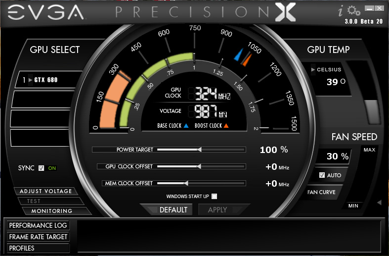
Finally, with the introduction of GPU Boost overclocking has been affected as well. Rather than directly controlling the core clock, overclocking is accomplished through the combined manipulation of the GPU Boost power target and the use of a GPU clock offset. Power target manipulation works almost exactly as you’d expect: you can lower and raise the GPU Boost power target by -30% to +32%, similar to how adjusting the PowerTune limit works on AMD cards. Increasing the power target allows the video card to pull more power, thereby allowing it to boost to higher steps than is normally possible (but no higher than the max step), while decreasing the power target keeps it from boosting at all.
The GPU offset meanwhile manipulates the steps themselves. By adjusting the GPU offset all of the GPU Boost steps are adjusted by roughly an equal amount, depending on what clocks the PLL driving the GPU can generate. E.G. a +100MHz offset clock would increase the 1st step to 1120MHz, etc up to the top step which would be increased to 1210MHz.
While each factor can be adjusted separately, it’s adjusting both factors together that truly unlock overclocking. Adjusting the GPU offset alone won’t achieve much if most workloads are limited by GPU Boost’s power target, and adjusting the power target alone won’t improve the performance of workloads that are already allowed to reach the highest step. By combining the two you can increase the GPU clock and at the same time increase the power target so that workloads are actually allowed to hit those new clocks.
On that note, overclocking utilities will be adding support for GPU Boost over the coming weeks. The first overclocking utility with support for GPU Boost is EVGA’s Precision X, the latest rendition of their Precision overclocking utility. NVIDIA supplied Precision X Beta 20 with our review samples, and as we understand it that will be made available shortly for GTX 680 buyers.
Finally, while we’ll go into full detail on overclocked performance in a bit, we wanted to quickly showcase the impact GPU Boost, both on regular performance and on overclocking. First up, we ran all of our benchmarks at 2560 with the power target for GPU boost set to -16%, which reduces the power target to roughly 142W. While GPU Boost cannot be disabled outright, this was enough to ensure that it almost never activated.
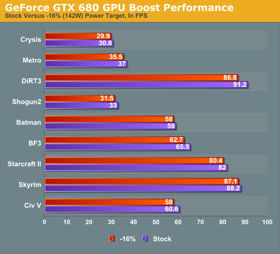
As is to be expected, the impact of GPU Boost varies depending on the game, but overall we found that enabling GPU boost on our card only improves performance by an average of 3%, and by no more than 5%. While this is effectively free performance, it also is a stark reminder that GPU Boost isn’t nearly as potent as turboing on a CPU – at least not quite yet. As there’s no real equivalent to the lightly threaded workload for GPUs, the need for a wide range of potential GPU Boost clocks is not nearly as great as the need for high turbo clocks on a CPU. Even a light GPU workload is relatively heavy when graphics itself is an embarrassingly parallel task.
Our other quick look is at overclocking. The following is what our performance looked like at 2560 with stock GPU Boost settings, a power target of +16% (195W), and a GPU offset of +100MHz.
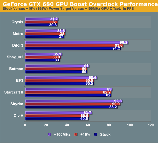
Overall raising the GPU offset is much more effective than raising the power target to improve performance, reflecting the fact that in our case most games were limited by the GPU Boost clock rather than the power target at least some of the time.


404 Comments
View All Comments
sngbrdb - Friday, March 30, 2012 - link
*from : PMombasa69 - Wednesday, April 4, 2012 - link
This is just a rebadged mid-range card, the 680 has less memory bandwidth than GPU's brought out 4 years ago lol, what a ripp, I can see the big fat directors at Nvidia laughing at all the mugs that have gone out and bought one, thinking this is the real big boy to replace the 580... muppets. lol.N4v1N - Wednesday, April 4, 2012 - link
Nvidia is the bestest! No AMD is the betterest!lol...
CeriseCogburn - Friday, April 6, 2012 - link
Yes Nvidia clocked the ram over 6Ghz because their ram controller is so rockin'.In any case, the 7970 is now being overclocked, both are to 7000Ghz ram.
Unfortunately the 7970 still winds up behind most of the time, even in 2650X1200 screen triple gaming.
raghu78 - Saturday, April 7, 2012 - link
In the Reference Radeon HD 7970 AND XFX RADEON HD 7970 review the DirectX 11 compute shader Fluid simulation perfomance is far more than in this review.http://www.anandtech.com/show/5261/amd-radeon-hd-7...
http://www.anandtech.com/show/5314/xfxs-radeon-hd-...
http://images.anandtech.com/graphs/graph5314/43383...
Reference HD 7970 -133 and XFX HD 7970 -145 . In this review Reference HD 7970 -115.5
What has changed in between these reviews. Is it that performance has actually decreased with the latest drivers
oddnutz - Thursday, April 12, 2012 - link
well i have been an ATI fanboi forever. So I am due a gfx upgrade which would of already happened if ATI priced their latest cards similar to previous generations. I will watch ATI prices over the next few weeks but it looks like i might be turning green soon.blanarahul - Friday, April 13, 2012 - link
Actually the GTX 680 REFERENCE BOARD was designed for 375 Watts of power.It has a total of 2 6-pin and one 8-pin connector on the board! I realized this after seeing the back of the board.
Commander Bubble - Thursday, April 19, 2012 - link
I agree with some of the sensible posts littered in here that Witcher 2 should be included as a comparison point, and most notably the ubersampling setup.i run 2x 580GTX SLI @1920 and i can't manage a minimum 60fps with that turned on. That would be a good test for current cards as it absoultely hammers them.
also, i don't know whether CeriseCogburn is right or wrong, and i don't care, but i'm just sick of seeing his name in the comment list. go outside and meet people, do something else. you are clearly spending way too much time on here...
beiker44 - Tuesday, April 24, 2012 - link
I can't wait to get one...or wait for the bad ace Dual 690!!! decisions decisionsOxford Guy - Thursday, July 5, 2012 - link
"At the end of the day NVIDIA already had a strong architecture in Fermi, so with Kepler they’ve gone and done the most logical thing to improve their performance: they’ve simply doubled Fermi."Fermi Lite, you mean.
"Now how does the GTX 680 fare in load noise? The answer depends on what you want to compare it to. Compared to the GTX 580, the GTX 680 is practically tied – no better and no worse – which reflects NVIDIA’s continued use of a conservative cooling strategy that favors noise over temperatures."
No, the 680's cooling performance is inferior because it doesn't use a vapor chamber. Nvidia skimped on the cooling to save money, it seems.