The Xeon E5-2600: Dual Sandy Bridge for Servers
by Johan De Gelas on March 6, 2012 9:27 AM EST- Posted in
- IT Computing
- Virtualization
- Xeon
- Opteron
- Cloud Computing
Rendering Performance: Cinebench
Cinebench, based on MAXON's CINEMA 4D software, is probably one of the most popular benchmarks around as it is pretty easy to perform this benchmark on your own home machine. The benchmark supports 64 threads, more than enough for our 24- and 32-thread test servers. First we tested single-threaded performance, to evaluate the performance of each core.
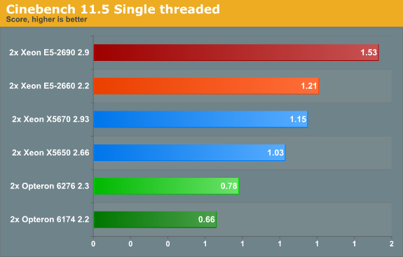
Cinebench achieves an IPC between 1.4 and 1.8 and is mostly dominated by SSE2 code. The Sandy Bridge core offers about 33% better single-threaded SSE performance. We checked: the 33% can be split up into 21% gains from architectural improvements and 12% from the improved Turbo capabilities.
Let's check out the multi-threaded score.
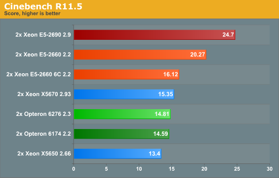
Prior to the launch of the Xeon E5 series, the Opteron 6276 offered a better performance per dollar ratio than comparable Xeon 5600s due to their similar performance at a much lower pricepoint. Now that the Xeon E5 has arrived, the tables have turned. If Xeon E5 servers are in the same price range as Xeon 5600 servers, the Xeon E5-2630 will offer the best performance/price ratio.
And if you want top performance, Intel is the only option. Case in point: a dual Xeon E5-2690 comes close to what a Quad Opteron 6276 can deliver, with the dual Xeon scoring 24.7 while the quad Opteron scores 26.4.


81 Comments
View All Comments
BSMonitor - Tuesday, March 6, 2012 - link
My question as well.What is the Intel roadmap for Ivy Bridge in this arena. Would be the same timeframe as IVB-E I would guess.
Wondering if my Intel dividends will pile up enough for me to afford one! Haha
devdeepc - Friday, September 2, 2016 - link
Based on the paper specs, AMD's 6276, 6274 and Intel's 2640 and 2630 are in a neck-and-neck race.fredisdead - Saturday, April 7, 2012 - link
From the 'article' .....'The Opteron might also have a role in the low end, price sensitive HPC market, where it still performs very well. It won't have much of chance in the high end clustered one as Intel has the faster and more power efficient PCIe interface'
Well, if that's the case, why exactly would AMD be scoring so many design wins with Interlagos. Including this one ...
http://www.pcmag.com/article2/0,2817,2394515,00.as...
http://www.eweek.com/c/a/IT-Infrastructure/Cray-Ti...
U think those guys at Cray were going for low performance ? In fact, seems like AMD has being rather cleaning up in the HPC market since the arrival of Interlagos. And the markets have picked up on it, AMD stock is thru the roof since the start of the year. Or just see how many Intel processors occupy the the top 10 supercomputers on the planet. Nuff said ...
iwod - Tuesday, March 6, 2012 - link
And not find a single comment on how and why "making this CPU quite a challenge, even for Intel."In my view It seems Intel is now using Server Market and Atom / SoC for their 32nm capacity when ever they introduce a new node in consumer products.
extide - Tuesday, March 6, 2012 - link
A large part of Intel's long-term strategies include keeping the fabs occupied.Latest gen fabs (currently 22nm) produce bleeding edge cpu's, usually in the consumer space
One gen back (32nm) produces server/workstation/mobile cpus
two gens back (45nm) produces other things like chipsets, and possibly itanium chips
even three gens back (65nm) probably still exists in some places making some chipsets as well.
Their goal is to as much use as possible from their investment into building the fabs themselves.
Kevin G - Tuesday, March 6, 2012 - link
65 nm is still used for Itanium, though the Poulson chip is due sometime this year made on a 32 nm process. If you want to compare die sizes, the 65 nm Tukwila design is 699 mm^2 in size.The main reason why 32 nm Sandybridge-E has been released so close to the release of 22 nm Ivy Bridge chips is that the initial Ivy Bridge chips are consumer centric. Intel performs additional testing on its server centric designs. This is particularly true as Sandybridge-E is not just replacing the dual socket Westmere-EP chips but some of the quad socket Westmere-EX market. RAS demands jump from going from dual to quad socket and that is reflected in additional testing. Implementing PCI-E 3.0 and QPI 1.1 also contributed to the time for additional testing.
Though you are correct that Intel does uses its older process nodes for various chipsets and IO chips. However, as Intel is marching toward SoC designs, the actual utility of keeping these older process nodes in action is decreasing.
meloz - Tuesday, March 6, 2012 - link
>And not find a single comment on how and why "making this CPU quite a challenge, even for Intel."Because it is such a massive die? 416 mm²? Large dies usually have a lower yield, and Intel's 32 nm process is still cutting edge (if only for a few more weeks, heh).
Look at how TSMC, Global Flounderings et al are struggling. An impressive achievement by Intel.
MrSpadge - Tuesday, March 6, 2012 - link
A significant amount of functionality has been added to the SB cores, and Intel can't afford mistakes in such CPUs.BSMonitor - Tuesday, March 6, 2012 - link
More than that though, the SNB-E, Xeon E cores are not duplicates of the SNB desktop cores.Look at Anand's die shot of SNB-E, vs die shot of SNB. The CPU cores, L3 cache, controllers, are arranged completely different. Which makes sense as SNB-E doesn't have to deal with 40% of the die being GPU transistors. So, what we have now with Intel is two completely different dies between Xeon/SNB-E and Core. The individual CPU cores are the same, but the rest of the die is completely different.
SNB-E:
http://www.anandtech.com/show/5091/intel-core-i7-3...
SNB:
http://www.anandtech.com/show/4083/the-sandy-bridg...
cynic783 - Tuesday, March 6, 2012 - link
omg these benches are so biased it's not even funny. everyone knows amd offers clock-for-clock more punch than intel and lower power as well