Intel's Medfield & Atom Z2460 Arrive for Smartphones: It's Finally Here
by Anand Lal Shimpi on January 10, 2012 8:00 PM ESTThe CPU
Medfield is the platform, Penwell is the SoC and the CPU inside Penwell is codenamed Saltwell. It's honestly not much different than the Bonnell core used in the original Atom, although it does have some tweaks for both power and performance.
Almost five years ago I wrote a piece on the architecture of Intel's Atom. Luckily (for me, not Intel), Atom's architecture hasn't really changed over the years so you can still look back at that article and have a good idea of what is at the core of Medfield/Penwell. Atom is still a dual-issue, in-order architecture with Hyper Threading support. The integer pipeline is sixteen stages long, significantly deeper than the Cortex A9's. The longer pipeline was introduced to help reduce Atom's power consumption by lengthening some of the decode stages and increasing cache latency to avoid burning through the core's power budget. Atom's architects, similar to those who worked on Nehalem, had the same 2:1 mandate: every new feature added to the processor's design had to deliver at least a 2% increase in performance for every 1% increase in power consumption.
Atom is a very narrow core as the diagram below will show:
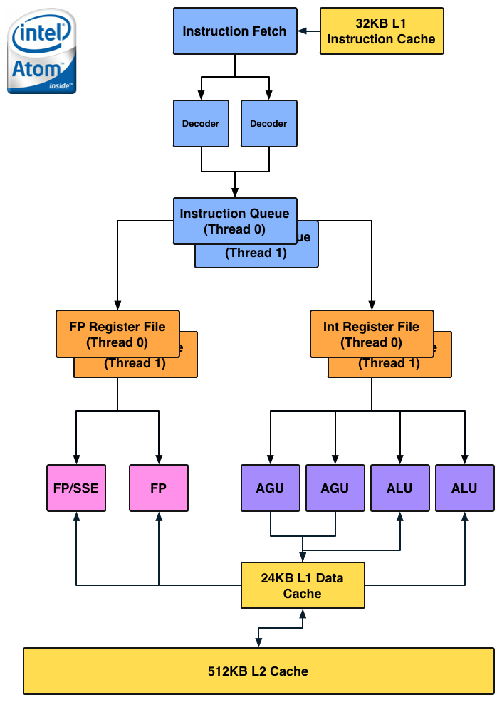
There are no dedicated integer multiply or divide units, that's all shared with the FP hardware. Intel duplicated some resources (e.g. register files, queues) to enable Hyper Threading support, but stopped short of increasing execution hardware to drive up efficiency. The tradeoff seems to have worked because Intel is able to deliver performance better than a dual-core Cortex A9 from a single HT enabled core. Intel also lucks out because while Android is very well threaded, not all tasks will continually peg both cores in a dual-core A9 machine. At higher clock speeds (1.5GHz+) and with heavy multi-threaded workloads, it's possible that a dual-core Cortex A9 could outperform (or at least equal) Medfield but I don't believe that's a realistic scenario.
Architecturally the Cortex A9 doesn't look very different from Atom:
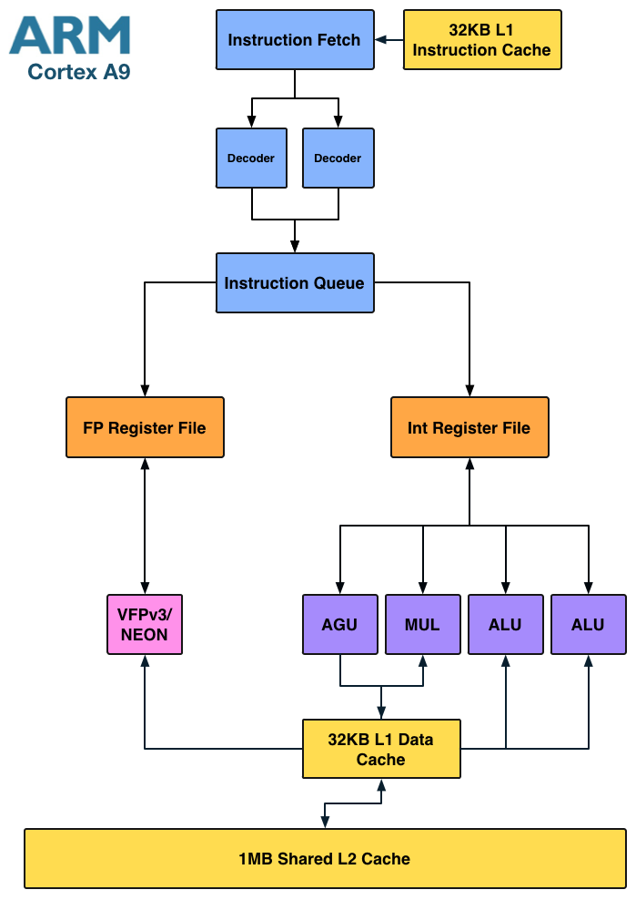
Here we see a dedicated integer multiply unit (shared with one of the ALU ports) but only a single port for FP/NEON. It's clear that the difference between Atom and the Cortex A9 isn't as obvious at the high level. Instead it's the lower level architectural decisions that gives Intel a performance advantage.
Where Intel is in trouble is if you look at the Cortex A15:
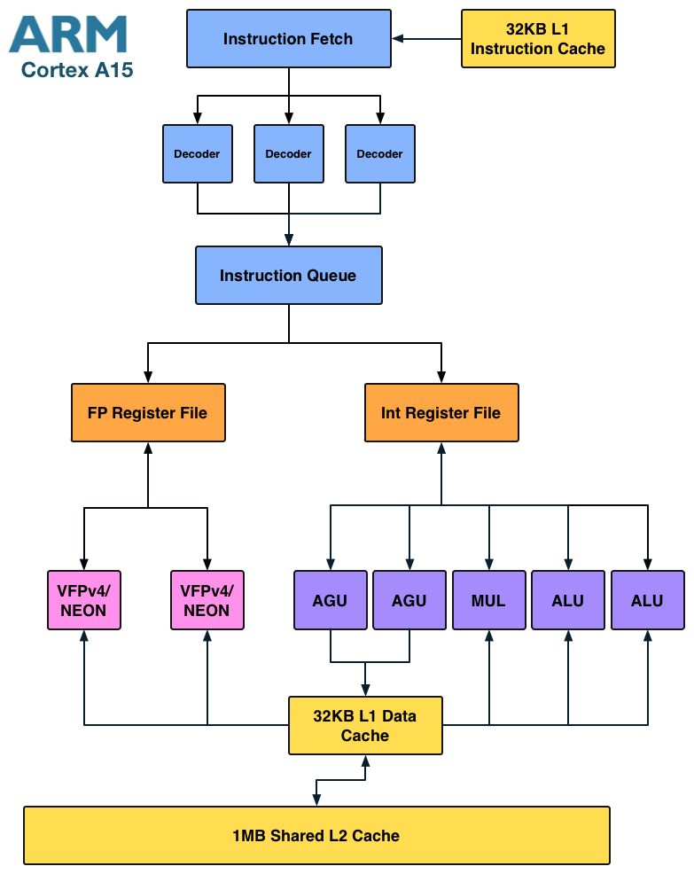
The A15 is a far more modern design, also out of order but much wider than A9. I fully expect that something A15-class can outperform Medfield, especially if the former is in a dual-core configuration. Krait falls under the A15-class umbrella so I believe Medfield has the potential to lose its CPU performance advantage within a couple of quarters.
Enhancements in Saltwell
Although the CPU core is mated to a 512KB L2 cache, there's a separate 256KB low power SRAM that runs on its own voltage plane. This ULP SRAM holds CPU state and data from the L2 cache when the CPU is power gated in the deepest sleep state. The reasoning for the separate voltage plane is simple. Intel's architects found that the minimum voltage for the core was limited by Vmin for the ULP SRAM. By putting the two on separate voltage planes it allowed Intel to bring the CPU core down to a lower minimum power state as Vmin for the L2 is higher than it is for the CPU core itself. The downside to multiple power islands is an increase in die area. Since Medfield is built on Intel's 32nm LP process while the company transitions to 22nm, spending a little more on die area to build more power efficient SoCs isn't such a big deal. Furthermore, Intel is used to building much larger chips, making Medfield's size a relative nonissue for the company.
The die size is actually very telling as it's a larger SoC than a Tegra 2 with two Cortex A9s despite only featuring a single core. Granted the rest of the blocks around the core are different, but it goes to show you that the CPU core itself (or number of cores) isn't the only determination of the die size of an SoC.
The performance tweaks come from the usual learnings that take place over the course of any architecture's lifespan. Some instruction scheduling restrictions have been lifted, memory copy performance is up, branch predictor size increased and some microcode flows run faster on Saltwell now.
Clock Speeds & Turbo
Medfield's CPU core supports several different operating frequencies and power modes. At the lowest level is its C6 state. Here the core and L2 cache are both power gated with their state is saved off in a lower power on-die SRAM. Total power consumption in C6 of the processor island is effectively zero. This isn't anything new, Intel has implemented similar technologies in desktops since 2008 (Nehalem) and notebooks since 2010 (Arrandale).
When the CPU is actually awake and doing something however it has a range of available frequencies: 100MHz all the way up to 1.6GHz in 100MHz increments.
The 1.6GHz state is a burst state and shouldn't be sustained for long periods of time, similar to how Turbo Boost works on Sandy Bridge desktop/notebook CPUs. The default maximum clock speed is 1.3GHz, although just as is the case with Turbo enabled desktop chips, you can expect to see frequencies greater than 1.3GHz on a fairly regular basis.
Power consumption along the curve is all very reasonable:
| Medfield CPU Frequency vs. Power | ||||||
| 100MHz | 600MHz | 1.3GHz | 1.6GHz | |||
| SoC Power Consumption | ~50mW | ~175mW | ~500mW | ~750mW | ||
Since most ARM based SoCs draw somewhere below 1W under full load, these numbers seem to put Medfield in line with its ARM competitors - at least on the CPU side.
It's important to pay attention to the fact that we're dealing with similar clock frequencies to what other Cortex A9 vendors are currently shipping. Any performance advantages will either be due to Medfield boosting up to 1.6GHz for short periods of time, inherently higher IPC and/or a superior cache/memory interface.


164 Comments
View All Comments
Hector2 - Wednesday, January 11, 2012 - link
So you doubt Anand's power measurements too ?As for the DX11 demo, Intel's VP showed very poor judgement running a video when they had trouble getting the demo out in time -- that's a major screw up, but Anand showed that the hardware actually works in spite of the screwed up demo.
french toast - Thursday, January 12, 2012 - link
No i dont doubt Anands Integrity or his benchmarks, i have just questioned his optimistic assuptions on un proven Intel hardware, especially when Intel produced the scope and the power benchmarks.All of which compare last years hardware, all the Intel sorced benches are single threaded and are likely due to Intel software optimisations, and lastly because the atom is higher clocked.
The benches as exophase has pointed out are on things that the cpu is not loaded/stressed.
Its great he has provided us with an insight, but this in no way proves that this architecture is the best nor does it prove that it would have 'dominated' android devices last year for a whole number of reasons that i cant be bothered to re-type.
Anand has jumped the gun on his conclusions thats all im saying
Dark_Archonis - Tuesday, January 10, 2012 - link
Time for the haters to eat their words, and the ARM supporters to admit they were wrong.On the forums there were enough self-proclaimed "experts" that claimed Intel was doomed and that ARM would take over. Well who's laughing now? Here we see an Atom SoC, that has power characteristics EQUAL or BETTER THAN ARM SoCs, while posting very strong performance as well. This is keeping in mind that it is just the first step for Intel in the smartphone market.
ARM supporters are already claiming that Medfield only looks good because it's being compared to year-old ARM designs. But guess what, the Atom design is 5 years old! Yes, this is a new SoC for Intel, but the fact is Intel must be given HUGE credit that they were able to make an SoC based on the 5-year old Atom design that is extremely competitive in power and performance to ARM SoCs.
Next-gen ARM designs will arrive later this year yes, but Intel will not stand still either. Also lets not forget about the next-gen Atom that will come in 2013 on the 22nm process. That will be a HUGE leap forward for Intel and will put them in an extremely competitive position against any quad-core ARM SoCs.
DigitalFreak - Tuesday, January 10, 2012 - link
You want a cookie or something? No-one cares about your fanboy rant.Dark_Archonis - Tuesday, January 10, 2012 - link
Obviously you cared enough to login, and make a useless, childish post devoid of anything meaningful, instead of actually replying to what I had posted.Great job at proving yourself wrong.
name99 - Wednesday, January 11, 2012 - link
Dude, the reason he is (justifiably) mocking you is that you are comparing ARM silicon that is shipping TODAY with Intel silicon that will be shipping in a YEAR.That's how it works among adults --- you compare shipping with shipping, not what I plan to ship (one day) with what you plan to ship (one day).
guilmon19 - Tuesday, January 10, 2012 - link
Except that Medfield is built on a 32nm process while ALL available A9s out there are built on the 45nm process. If the A9's were 32nm as well these benchmarks would be very different and these benchmarks came straight from intel, lets way wait till we actually get the phone and do benchmarks from there to determine which one is better.madmilk - Tuesday, January 10, 2012 - link
Doesn't matter than Medfield is 32nm, by the time anyone else makes a 32nm SoC Intel will be on 22nm.It's a massive advantage that can't just be thrown away, especially if trying to make a fair comparison.
Exophase - Tuesday, January 10, 2012 - link
Hardly, TSMC 28nm ARM processors are right around the corner while 22nm Atoms won't hit until 2013. Intel's doesn't yet have the same process advantage with their LP SoC nodes.Dark_Archonis - Tuesday, January 10, 2012 - link
Your point being? Even looking at TSMC's 28nm process, Intel will still have quite an advantage with their 22nm process. ARM will only have an advantage for a few quarters with the 28nm process, then Intel will come out with their 22nm process. You also fail to acknowledge that Atom on 22nm (Silvermont) will a brand new Atom architecture, which you can bet will be a HUGE leap forward in performance and power efficiency.TSMC is well known for having lots of trouble moving to new a process. Exophase, you should rephrase "right around the corner" to say in 1-2 quarters at the very least. It will still be a few months before we see any 28nm ARM phones actually on the market.
Intel has aligned their mobile and desktop process roadmaps, so all future Atoms will move to a new process node as fast as Intel's desktop chips.
Intel will also have a technological advantage as their 22nm process introduces FinFET, while TSMC won't have FinFET until their 14nm process.
Furthermore, Intel intends to introduce 14nm in 2013/2014, while TSMC won't introduce 14nm until 2015.
Intel was really slow getting into the smartphone market, but now that they have their foot in the door, they will not let off the gas. Intel's efforts in the smartphone market will only accelerate from this point. Intel will attack ARM directly at the low-end power scale in this case, and ARM will struggle greatly at the high end as Intel's Haswell will offer revolutionary power/performance ratios. That's not even mentioning what power/performance ratios we will see from the the next-gen Atom design.
Also let me restate that this is Intel's *first step* into the smartphone market, and they are able to be very competitive with ARM designs.