Intel Core i7 3960X (Sandy Bridge E) Review: Keeping the High End Alive
by Anand Lal Shimpi on November 14, 2011 3:01 AM EST- Posted in
- CPUs
- Intel
- Core i7
- Sandy Bridge
- Sandy Bridge E
Final Words
There are two aspects of today's launch that bother me: the lack of Quick Sync and the chipset. The former is easy to understand. Sandy Bridge E is supposed to be a no-compromise, ultra high-end desktop solution. The lack of an on-die GPU with Quick Sync support means you have to inherently compromise in adopting the platform. I'm not sure what sort of a solution Intel could've come to (I wouldn't want to give up a pair of cores for a GPU+QuickSync) but I don't like performance/functionality tradeoffs with this class of product. Secondly, while I'm not a SAS user, I would've at least appreciated some more 6Gbps SATA ports on the chipset. Native USB 3.0 support would've been nice as well. Instead what we got was effectively a 6-series chipset with a new name. As Intel's flagship chipset, the X79 falls short.
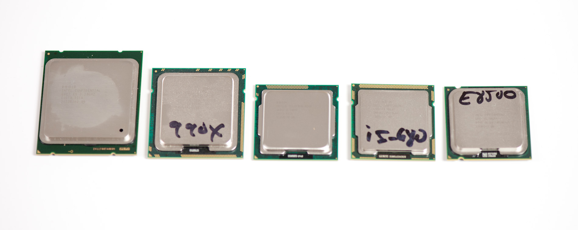
From left to right: Intel Core i7 (SNB-E), Core i7 (Gulftown), Core i5 (SNB), Core i5 (Clarkdale), Core 2 Duo
LGA-2011, 1366, 1155, 1156, 775
The vast majority of desktop users, even enthusiast-class users, will likely have no need for Sandy Bridge E. The Core i7 3960X may be the world's fastest desktop CPU, but it really requires a heavily threaded workload to prove it. What the 3960X doesn't do is make your gaming experience any better or speed up the majority of desktop applications. The 3960X won't be any slower than the fastest Sandy Bridge CPUs, but it won't be tremendously faster either. The desktop market is clearly well served by Intel's LGA-1155 platform (and its lineage); LGA-2011 is simply a platform for users who need a true powerhouse.
There are no surprises there, we came to the same conclusion when we reviewed Intel's first 6-core CPU last year. If you do happen to have a heavily threaded workload that needs the absolute best performance, the Core i7 3960X can deliver. In our most thread heavy tests the 3960X had no problems outpacing the Core i7 2600K by over 50%. If your livelihood depends on it, the 3960X is worth its entry fee. I suspect for those same workloads, the 3930K will be a good balance of price/performance despite having a smaller L3 cache. I'm not terribly interested in next year's Core i7 3820. Its point is obviously for those users who need the memory bandwidth or PCIe lanes of SNB-E, but don't need more than four cores. I would've liked to have seen a value 6-core offering instead, but I guess with a 435mm2 die size it's a tough sell for Intel management.

Of course compute isn't the only advantage of the Sandy Bridge E platform. With eight DIMM slots on most high end LGA-2011 motherboards you'll be able to throw tons of memory at your system if you need it without having to shop for workstation motherboards with fewer frills.
As for the future of the platform, Intel has already begun talking about Ivy Bridge E. If it follows the pattern set for Ivy Bridge on LGA-1155, IVB-E should be a drop in replacement for LGA-2011 motherboards. The biggest issue there is timing. Ivy will arrive for the mainstream LGA-1155 platforms around the middle of 2012. At earliest, I don't know that we'd see it for LGA-2011 until the end of next year, or perhaps even early 2013 given the late launch of SNB-E. This seems to be the long-term downside to these ultra high-end desktop platforms these days: you end up on a delayed release cadence for each tick/tock on the roadmap. If you've always got to have the latest and greatest, this may prove to be frustrating. Based on what we know of Ivy Bridge however, I suspect that if you're using all six of these cores in SNB-E that you'll wish you had IVB-E sooner, but won't be tempted away from the platform by a quad-core Ivy Bridge on LGA-1155.
I do worry about the long term viability of the ultra high-end desktop platform. As we showed here, some of the gains in threaded apps exceed 50% over a standard Sandy Bridge. That's tangible performance to those who can use it. With the growth in cloud computing it's clear there's demand for these types of chips in servers. I just hope Intel continues to offer a version for desktop users as well.


163 Comments
View All Comments
jabber - Monday, November 14, 2011 - link
...with Pixar updating their rendering farm?I cant think of many other big customers for this kind of chip.
randinspace - Monday, November 14, 2011 - link
Wouldn't they be using Xeons?gevorg - Monday, November 14, 2011 - link
Could the wasted space for 2 fused cores and their L3 cache been used for HD2000 graphics? Wish Intel would have avoided wasting die space like this.GL1zdA - Monday, November 14, 2011 - link
It's not wasting, it's binning. They could either throw away 8-cores with damaged cores or sell them as six-cores, which is what they did.BSMonitor - Monday, November 14, 2011 - link
Actually it's not binning in this case. (some chips from the Xeon line might be) But these "desktop" CPUs are actually the 8-core Xeon line trimmed down in both cost and validation for use in Desktop PCs. Intel's currently roadmap is 6-core desktop CPU's at the high-end with extremely high memory bandwidth.It is cheaper for them to fuse two cores from an 8-core Xeon production line, than to redesign another CPU die for just the high-end 6-core desktop line. This class is by no means high-volume, hence yet another CPU die would be expensive.
GL1zdA - Monday, November 14, 2011 - link
Could you test how Sandy Bridge-E behaves in vt_benchmark when GPU trancoding is used? I'm curious, if SBE will do better than a nVidia 580. And what is the difference between 2600K+580 and 3960X+580 when GPU transcoding is enabled.Kevin G - Monday, November 14, 2011 - link
Intel crippled both the CPU and the chipset with this launch. I was hoping to see an 8 core model at the high end. The chip design itself is an 8 core die so why not a fully functional chip for the low volume extreme edition? The performance benefits of the Core i7 3960X over the 990X mirror those from the 2600K over the 875K. (Well actually the 2600K vs. 875K comparison is much wider due to the clock speed differences, not just the architectural changes.) Sure it is faster at stock but generally not worth upgrading to, especially factoring in motherboard cost. Another let down is that the chip doesn't officially support PCI-E 3.0 True that their are no PCI-E 3.0 cards on the market today but there will be tomorrow. Not sure if this is additional crippling to distinguish the consumer chips from the coming LGA2011 Xeons or if there actually was a problem running at PCI-E 3.0 speeds.Speaking of Xeons, this article didn't mention if the system has the two QPI links disabled. If not, there could be the remote chance of a manufacturer releasing a board with the X79 using DMI and an X58 chipset hanging off of a QPI link. That would allow for another two full bandwidth PCI-E 16X slots at 2.0 speeds without the usage of a bridge chip.
Then there is the X79 chipset. The reality is that it offers very little over the Z68. No USB 3.0 or additional SATA ports are the big things. Knowing Intel, we'll likely see a Z79 chipset that'll enable the SAS functionality for those that want more storage. Hopefully the hypothetical Z79 chipset will also use some of the PCI-E lanes from the CPU for additional bandwidth as an array of SSD's would easily be able to saturate the current DMI link.
I'm also curious if these X79 consumer boards will allow for some overclocking with an LGA 2011 Xeon. I'm not expected full multiplier controller but rather feeding that 125 Mhz or 166 Mhz base clock to the CPU would suffice. Getting one of these consumer boards and paying the Xeon premium may wind up being the way to go for a true leap over of the Core i7 990X.
khanov - Monday, November 14, 2011 - link
This is a good question, I guess many would wonder why this is the case. To understand why requires a little insight into the manufacturing of silicon chips:
As with almost any manufacturing process there are variables that differentiate one product coming off the same assembly line from the next. So for example at a car factory each 'identical' engine is in fact a little different from another, whether it be the balancing of the crankshaft or the exact fit of the bearings.
With the manufacturing of CPUs (and indeed any silicon chips) there are also small differences between the chips that come off the same assembly line. If a chip has a defect for example (which happens too frequently) the defective area of the chip needs to be disabled. In essence this is why we are seeing Sandy Bridge-E cpus launching with disabled cores.
The fully enabled cores (eight cores and 20MB L3 cache) are being sold as (or will soon be sold as) Xeon chips for the highest price. Somewhat lesser cores with defects are being sold as lower end Xeons with six cores or as consumer Sandy Bridge-E chips with six cores. Even more defective chips that can only work with four cores enabled are being stockpiled and will soon be sold as four core Sandy-Bridge-E and Xeon chips.
So basically all these chips are manufactured with eight 'possible' cores. There is no wasted space on the die. However due to imperfect manufacturing processes some of these chips will have defects. In fact the larger the die area the more likely a defect occurs within each chip. With a very large die area for SB-E intel is now experiencing a problem more often seen by GPU manufacturers such as Nvidia. They are dealing with the problem in the same way: While Nvidia sell a GTX580 with die defects as a GXT570, intel sells a defective 8 core SB-E as a fully working 6 core Xeon or SB-E chip.
Once we see an improvement of the manufacturing process (which is an ongoing process of improvement) we will start to see lower cost SB-E chips and also possibly fully enabled, defect-free SB-E for desktop/workstation users.
javalino - Monday, November 14, 2011 - link
AGREE!!!!I will wait for a native 6 core, it will be much cooler , and maybe 1% fasterkarakarga - Monday, November 14, 2011 - link
Hi,From i386 DX-40 times, AMD build it's worst CPU ever. With 2 Billion transistors, instead of 0,9 Billion transistors. Typically new Bulldozer architecture have not much effect. So they doubled the transistor count for nothing! A very poor design. I am thinking AMD FX-8150 is not an eight core but considering new AMD bullozer 8C CPU as a 4 core but 8 threaded. Intel here reached 2,3 Billion transistors. But the performance is about 1,5 times better than AMD.
Chipset details are known. The lack of having only two SATA-600 ports is a disadvantage. Lack of native USB 3.0 support prevents mainboards fully passing to the new speed standard.
But AMD is also not good at chipset design too. I am currently using 990FX chipset with 1090T cpu. The memory performance is not reaching to 10GB/s with four DDR3-2133 rams working at 1600MHz default. If I put this CPU on a 790FX mainboard with only two piece DDR2-1066 rams, it passes 13GB/s. Which means the old serie upto 1100T are designed for DDR2 and not poolished and optimized fine for DDR3 memory. Only advantage here is having 6 SATA-600 ports, thats all!