Intel Core i7 3960X (Sandy Bridge E) Review: Keeping the High End Alive
by Anand Lal Shimpi on November 14, 2011 3:01 AM EST- Posted in
- CPUs
- Intel
- Core i7
- Sandy Bridge
- Sandy Bridge E
Windows 7 Application Performance
3dsmax 9
Today's desktop processors are more than fast enough to do professional level 3D rendering at home. To look at performance under 3dsmax we ran the SPECapc 3dsmax 8 benchmark (only the CPU rendering tests) under 3dsmax 9 SP1. The results reported are the rendering composite scores.
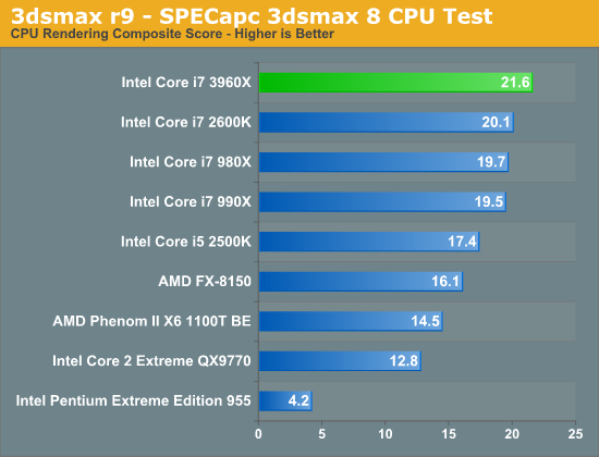
Offline 3D rendering applications make some of the best use of CPU cores, unfortunately our test here doesn't scale all that well. We only see a 7% increase over the 2600K. If we look at a more modern 3D workload however...
Cinebench 11.5
Created by the Cinema 4D folks we have Cinebench, a popular 3D rendering benchmark that gives us both single and multi-threaded 3D rendering results.
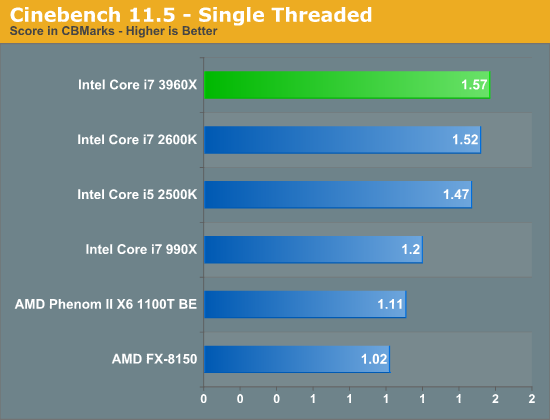
Single threaded performance is marginally better than the 2600K thanks to the 3960X's slightly higher max turbo speed. What's more important than the performance here is the fact that the 3960X is able to properly power gate all idle cores and give a single core full reign of the chip's TDP. Turbo is alive and well in SNB-E, just as it was in Sandy Bridge.
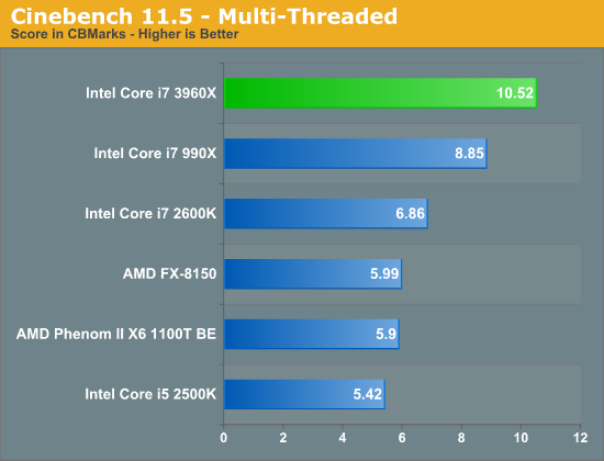
Here the performance gains are staggering. The 3960X is 53% faster than the 2600K and 19% faster than Intel's previous 6-core flagship, the 990X. The Bulldozer comparison is almost unfair, the 3960X is 75% faster (granted it is also multiple times the price of the FX-8150).
7-Zip Benchmark
While Cinebench shows us multithreaded floating point performance, the 7-zip benchmark gives us an indication of multithreaded integer performance:
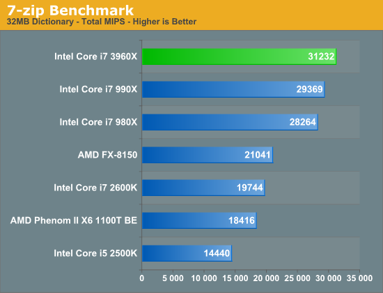
Here we see huge gains over the 2600K (58%), indicating that the increase in cache size and memory bandwidth help the boost in core count a bit here. The advantage over the 990X is only 7%. This gives us a bit of a preview of what we can expect from SNB-EP Xeon server performance.
PAR2 Benchmark
Par2 is an application used for reconstructing downloaded archives. It can generate parity data from a given archive and later use it to recover the archive
Chuchusoft took the source code of par2cmdline 0.4 and parallelized it using Intel’s Threading Building Blocks 2.1. The result is a version of par2cmdline that can spawn multiple threads to repair par2 archives. For this test we took a 708MB archive, corrupted nearly 60MB of it, and used the multithreaded par2cmdline to recover it. The scores reported are the repair and recover time in seconds.
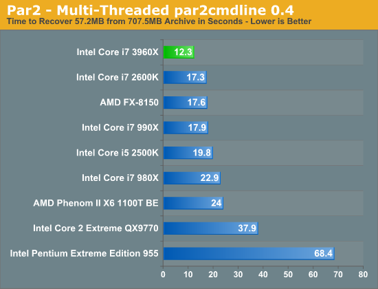
Here we see a 40% increase in performance over the 2600K and FX-8150.
TrueCrypt Benchmark
TrueCrypt is a very popular encryption package that offers full AES-NI support. The application also features a built-in encryption benchmark that we can use to measure CPU performance with:
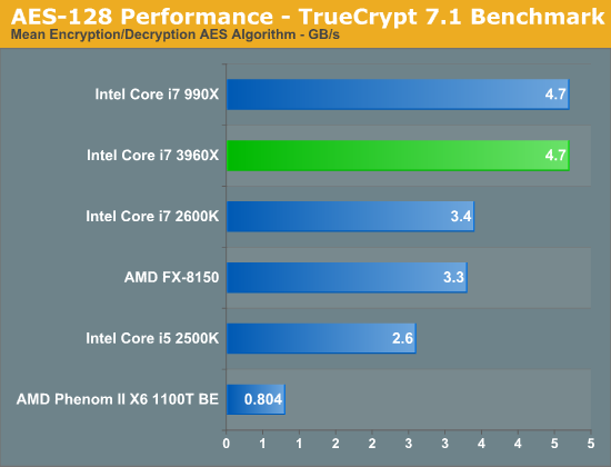
As both the 990X and 3960X have AES-NI support, both are equally capable at cranking through an AES workload. Per core performance doesn't appear to have changed all that much with the move to Sandy Bridge, so here we have a situation where the 3960X is much faster than the 2600K but no faster than the 990X. I suspect these types of scenarios will be fairly rare.
x264 HD 3.03 Benchmark
Graysky's x264 HD test uses x264 to encode a 4Mbps 720p MPEG-2 source. The focus here is on quality rather than speed, thus the benchmark uses a 2-pass encode and reports the average frame rate in each pass.
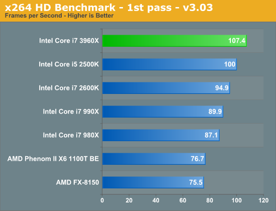
Single threaded performance isn't significantly faster than your run-of-the-mill Sandy Bridge, which means the first x264 HD pass doesn't look all that impressive on SNB-E.
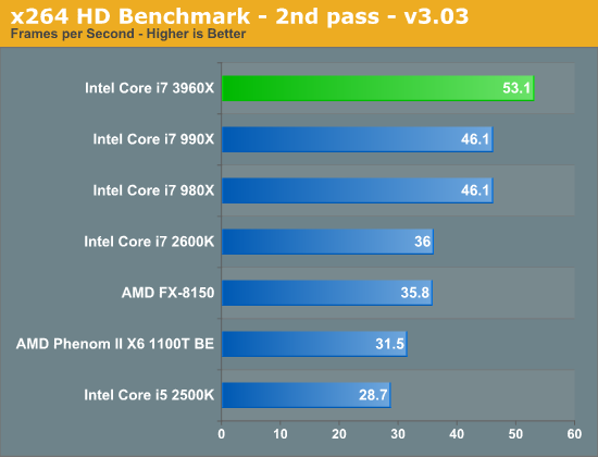
The second pass however stresses all six cores far more readily, resulting in a 47.5% increase in performance over the 2600K. Even compared to the 990X there's a 15% increase in performance.
Adobe Photoshop CS4
To measure performance under Photoshop CS4 we turn to the Retouch Artists’ Speed Test. The test does basic photo editing; there are a couple of color space conversions, many layer creations, color curve adjustment, image and canvas size adjustment, unsharp mask, and finally a gaussian blur performed on the entire image.
The whole process is timed and thanks to the use of Intel's X25-M SSD as our test bed hard drive, performance is far more predictable than back when we used to test on mechanical disks.
Time is reported in seconds and the lower numbers mean better performance. The test is multithreaded and can hit all four cores in a quad-core machine.
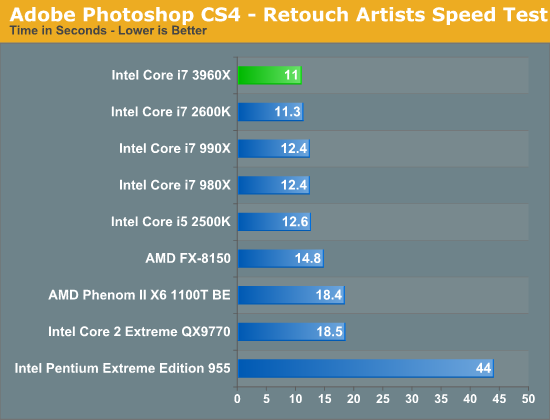
Our Photoshop test is multithreaded but there are only spikes that use more than four cores. That combined with the short duration of the benchmark shows no real advantage to the 3960X over the 2600K. Sandy Bridge E is faster than Intel's old 6-core solution though.
Compile Chromium Test
You guys asked for it and finally I have something I feel is a good software build test. Using Visual Studio 2008 I'm compiling Chromium. It's a pretty huge project that takes over forty minutes to compile from the command line on the Core i3 2100. But the results are repeatable and the compile process will stress all 12 threads at 100% for almost the entire time on a 980X so it works for me.
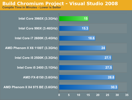
Our compile test is extremely well threaded, which once again does well on the 3960X. The gains aren't as big as what we saw in some of our earlier 3D/transcoding tests, but if you're looking to build the fastest development workstation you'll want a Sandy Bridge E.
Excel Monte Carlo
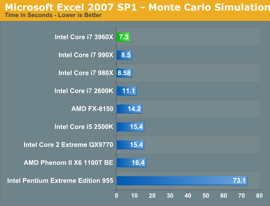
Multithreaded compute does well on SNB-E regardless of the type of application. Excel is multithreaded and if you have a beefy enough workload, you'll see huge gains over the 2600K.


163 Comments
View All Comments
jabber - Monday, November 14, 2011 - link
...with Pixar updating their rendering farm?I cant think of many other big customers for this kind of chip.
randinspace - Monday, November 14, 2011 - link
Wouldn't they be using Xeons?gevorg - Monday, November 14, 2011 - link
Could the wasted space for 2 fused cores and their L3 cache been used for HD2000 graphics? Wish Intel would have avoided wasting die space like this.GL1zdA - Monday, November 14, 2011 - link
It's not wasting, it's binning. They could either throw away 8-cores with damaged cores or sell them as six-cores, which is what they did.BSMonitor - Monday, November 14, 2011 - link
Actually it's not binning in this case. (some chips from the Xeon line might be) But these "desktop" CPUs are actually the 8-core Xeon line trimmed down in both cost and validation for use in Desktop PCs. Intel's currently roadmap is 6-core desktop CPU's at the high-end with extremely high memory bandwidth.It is cheaper for them to fuse two cores from an 8-core Xeon production line, than to redesign another CPU die for just the high-end 6-core desktop line. This class is by no means high-volume, hence yet another CPU die would be expensive.
GL1zdA - Monday, November 14, 2011 - link
Could you test how Sandy Bridge-E behaves in vt_benchmark when GPU trancoding is used? I'm curious, if SBE will do better than a nVidia 580. And what is the difference between 2600K+580 and 3960X+580 when GPU transcoding is enabled.Kevin G - Monday, November 14, 2011 - link
Intel crippled both the CPU and the chipset with this launch. I was hoping to see an 8 core model at the high end. The chip design itself is an 8 core die so why not a fully functional chip for the low volume extreme edition? The performance benefits of the Core i7 3960X over the 990X mirror those from the 2600K over the 875K. (Well actually the 2600K vs. 875K comparison is much wider due to the clock speed differences, not just the architectural changes.) Sure it is faster at stock but generally not worth upgrading to, especially factoring in motherboard cost. Another let down is that the chip doesn't officially support PCI-E 3.0 True that their are no PCI-E 3.0 cards on the market today but there will be tomorrow. Not sure if this is additional crippling to distinguish the consumer chips from the coming LGA2011 Xeons or if there actually was a problem running at PCI-E 3.0 speeds.Speaking of Xeons, this article didn't mention if the system has the two QPI links disabled. If not, there could be the remote chance of a manufacturer releasing a board with the X79 using DMI and an X58 chipset hanging off of a QPI link. That would allow for another two full bandwidth PCI-E 16X slots at 2.0 speeds without the usage of a bridge chip.
Then there is the X79 chipset. The reality is that it offers very little over the Z68. No USB 3.0 or additional SATA ports are the big things. Knowing Intel, we'll likely see a Z79 chipset that'll enable the SAS functionality for those that want more storage. Hopefully the hypothetical Z79 chipset will also use some of the PCI-E lanes from the CPU for additional bandwidth as an array of SSD's would easily be able to saturate the current DMI link.
I'm also curious if these X79 consumer boards will allow for some overclocking with an LGA 2011 Xeon. I'm not expected full multiplier controller but rather feeding that 125 Mhz or 166 Mhz base clock to the CPU would suffice. Getting one of these consumer boards and paying the Xeon premium may wind up being the way to go for a true leap over of the Core i7 990X.
khanov - Monday, November 14, 2011 - link
This is a good question, I guess many would wonder why this is the case. To understand why requires a little insight into the manufacturing of silicon chips:
As with almost any manufacturing process there are variables that differentiate one product coming off the same assembly line from the next. So for example at a car factory each 'identical' engine is in fact a little different from another, whether it be the balancing of the crankshaft or the exact fit of the bearings.
With the manufacturing of CPUs (and indeed any silicon chips) there are also small differences between the chips that come off the same assembly line. If a chip has a defect for example (which happens too frequently) the defective area of the chip needs to be disabled. In essence this is why we are seeing Sandy Bridge-E cpus launching with disabled cores.
The fully enabled cores (eight cores and 20MB L3 cache) are being sold as (or will soon be sold as) Xeon chips for the highest price. Somewhat lesser cores with defects are being sold as lower end Xeons with six cores or as consumer Sandy Bridge-E chips with six cores. Even more defective chips that can only work with four cores enabled are being stockpiled and will soon be sold as four core Sandy-Bridge-E and Xeon chips.
So basically all these chips are manufactured with eight 'possible' cores. There is no wasted space on the die. However due to imperfect manufacturing processes some of these chips will have defects. In fact the larger the die area the more likely a defect occurs within each chip. With a very large die area for SB-E intel is now experiencing a problem more often seen by GPU manufacturers such as Nvidia. They are dealing with the problem in the same way: While Nvidia sell a GTX580 with die defects as a GXT570, intel sells a defective 8 core SB-E as a fully working 6 core Xeon or SB-E chip.
Once we see an improvement of the manufacturing process (which is an ongoing process of improvement) we will start to see lower cost SB-E chips and also possibly fully enabled, defect-free SB-E for desktop/workstation users.
javalino - Monday, November 14, 2011 - link
AGREE!!!!I will wait for a native 6 core, it will be much cooler , and maybe 1% fasterkarakarga - Monday, November 14, 2011 - link
Hi,From i386 DX-40 times, AMD build it's worst CPU ever. With 2 Billion transistors, instead of 0,9 Billion transistors. Typically new Bulldozer architecture have not much effect. So they doubled the transistor count for nothing! A very poor design. I am thinking AMD FX-8150 is not an eight core but considering new AMD bullozer 8C CPU as a 4 core but 8 threaded. Intel here reached 2,3 Billion transistors. But the performance is about 1,5 times better than AMD.
Chipset details are known. The lack of having only two SATA-600 ports is a disadvantage. Lack of native USB 3.0 support prevents mainboards fully passing to the new speed standard.
But AMD is also not good at chipset design too. I am currently using 990FX chipset with 1090T cpu. The memory performance is not reaching to 10GB/s with four DDR3-2133 rams working at 1600MHz default. If I put this CPU on a 790FX mainboard with only two piece DDR2-1066 rams, it passes 13GB/s. Which means the old serie upto 1100T are designed for DDR2 and not poolished and optimized fine for DDR3 memory. Only advantage here is having 6 SATA-600 ports, thats all!