NVIDIA's Tegra 3 Launched: Architecture Revealed
by Anand Lal Shimpi on November 9, 2011 12:34 AM ESTThe Tegra 3 GPU: 2x Pixel Shader Hardware of Tegra 2
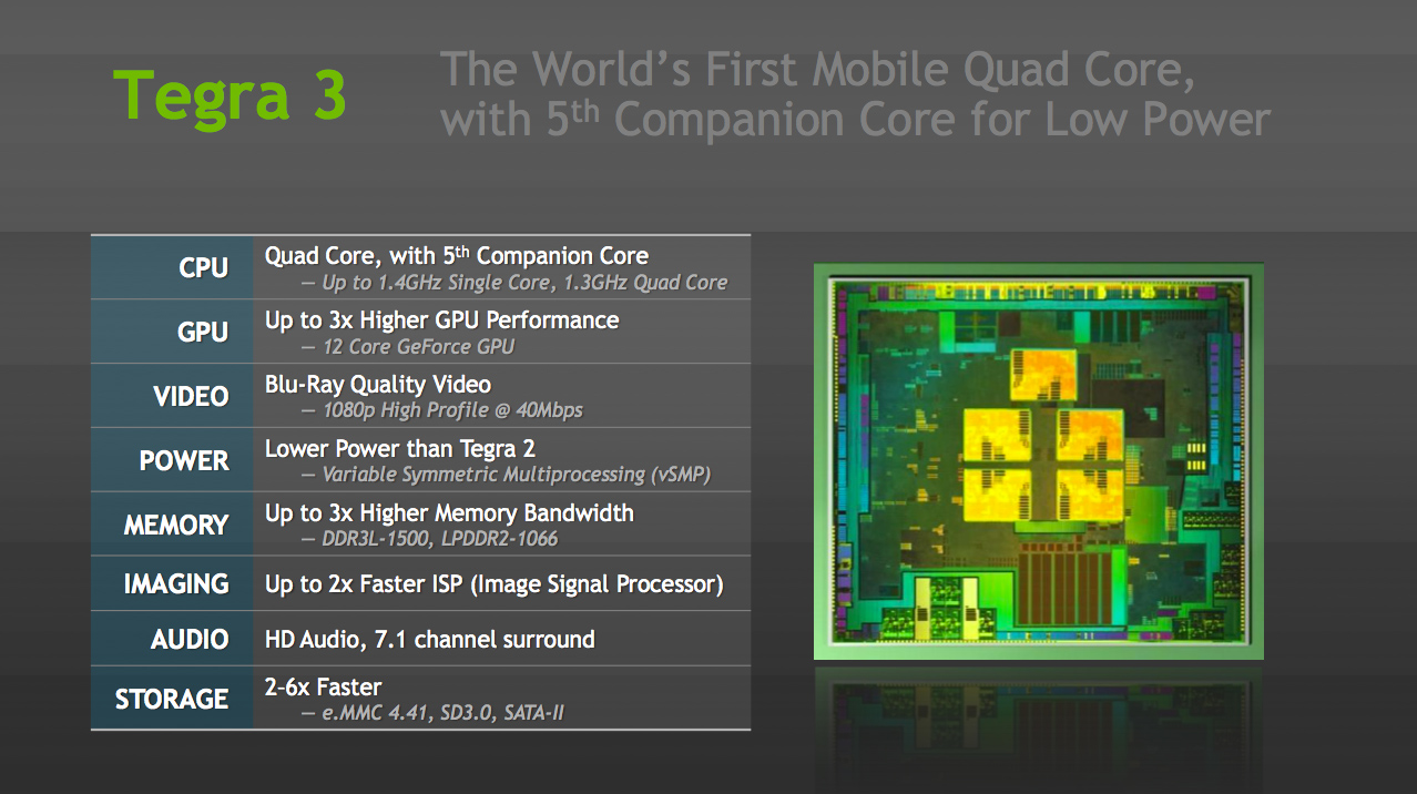
Tegra 3's GPU is very much an evolution of what we saw in Tegra 2. The GeForce in Tegra 2 featured four pixel shader units and four vertex shader units; in Tegra 3 the number of pixel shader units doubles while the vertex processors remain unchanged. This brings Tegra 3's GPU core count up to 12. NVIDIA still hasn't embraced a unified architecture, but given how closely it's mimicking the evolution of its PC GPUs I wouldn't expect such a move until the next-gen architecture - possibly in Wayne.
| Mobile SoC GPU Comparison | |||||||||||
| Adreno 225 | PowerVR SGX 540 | PowerVR SGX 543 | PowerVR SGX 543MP2 | Mali-400 MP4 | GeForce ULP | Kal-El GeForce | |||||
| SIMD Name | - | USSE | USSE2 | USSE2 | Core | Core | Core | ||||
| # of SIMDs | 8 | 4 | 4 | 8 | 4 + 1 | 8 | 12 | ||||
| MADs per SIMD | 4 | 2 | 4 | 4 | 4 / 2 | 1 | 1 | ||||
| Total MADs | 32 | 8 | 16 | 32 | 18 | 8 | 12 | ||||
| GFLOPS @ 200MHz | 12.8 GFLOPS | 3.2 GFLOPS | 6.4 GFLOPS | 12.8 GFLOPS | 7.2 GFLOPS | 3.2 GFLOPS | 4.8 GFLOPS | ||||
| GFLOPS @ 300MHz | 19.2 GFLOPS | 4.8 GFLOPS | 9.6 GFLOPS | 19.2 GFLOPS | 10.8 GFLOPS | 4.8 GFLOPS | 7.2 GFLOPS | ||||
Per core performance has improved a bit. NVIDIA worked on timing of critical paths through the GPU's execution units to help it run at higher clock speeds. NVIDIA wouldn't confirm the target clock for Tegra 3's GPU other than to say it was higher than Tegra 2's 300MHz. Peak floating point throughput per core is unchanged (one MAD per clock), but each core should be more efficient thanks to larger caches in the design.
A combination of these improvements as well as newer drivers are what give Tegra 3's GPU its 2x - 3x performance advantage over Tegra 2 despite only a 50% increase in overall execution resources. In pixel shader bound scenarios, there's an effective doubling of execution horsepower so the 2x gains are more believable there. I don't expect many games will be vertex processing bound so the lack of significant improvement there shouldn't be a big issue for Tegra 3.
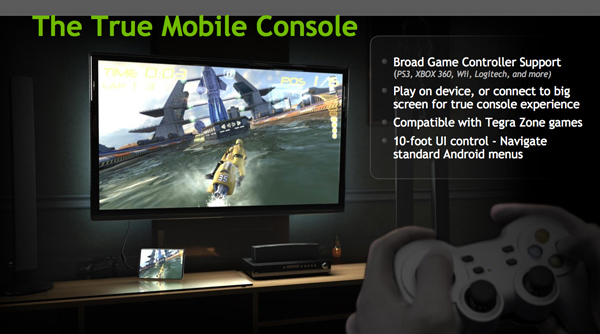
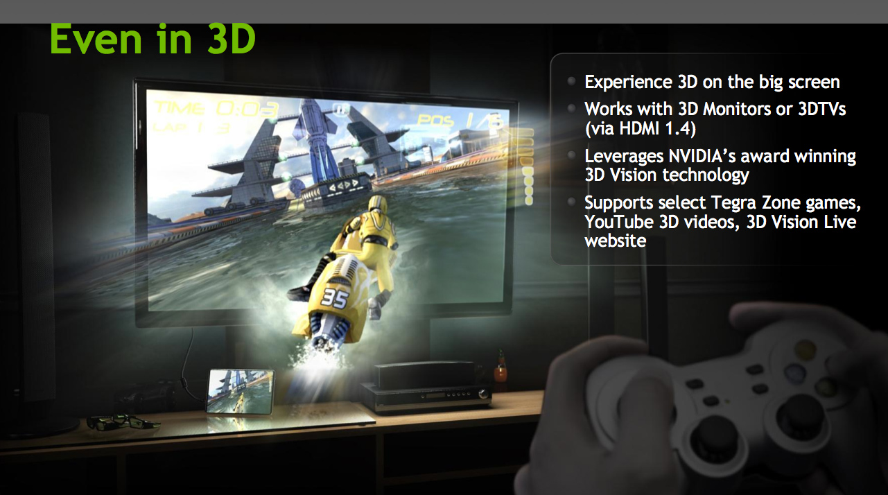
Ready for Gaming: Stereoscopic 3D and Expanded Controller Support
Tegra 3 now supports stereoscopic 3D for displaying content from YouTube, NVIDIA's own 3D Vision Live website and some Tegra Zone games. In its port of Android, NVIDIA has also added expanded controller support for PS3, Xbox 360 and Wii controllers among others.
Tegra 3 Video Encoding/Decoding and ISP
There's unfortunately not too much to go on here, especially not until we have some testable hardware in hand, but NVIDIA is claiming a much improved video decoder and more efficient video encoder in Tegra 3.
Tegra 3's video decoder can accelerate 1080p H.264 high profile content at up to 40Mbps, although device vendors can impose their own bitrate caps and file limitations on the silicon. NVIDIA wouldn't go into greater detail as to what's changed since Tegra 2, other than to say that the video decoder is more efficient. The video encoder is capable of 1080p H.264 base profile encode at 30 fps.
The Image Signal Processor (ISP) in Tegra 3 is twice as fast as what was in Tegra 2 and NVIDIA promised more details would be forthcoming (likely alongside the first Tegra 3 smartphone announcements).
Memory Interface: Still Single Channel, DDR3L-1500 Supported
Tegra 3 supports higher frequency memories than Tegra 2 did, but the memory controller itself is mostly unchanged from the previous design. While Tegra 2 supported LPDDR2 at data rates of up to 600MHz, Tegra 3 increases that to LPDDR2-1066 and DDR3-L is supported at data rates of up to 1500MHz. The memory interface is still only 32-bits wide, resulting in far less theoretical bandwidth than Apple's A5, Samsung's Exynos 4210, TI's OMAP 4, or Qualcomm's upcoming MSM8960. This is particularly concerning given the increase in core count as well as GPU execution resources. NVIDIA doesn't expect memory bandwidth to be a limitation, but I can't see how that wouldn't be the case in 3D games. Perhaps it's a good thing that Infinity Blade doesn't yet exist for Android.
SATA II Controller: On Die
Given Tegra 3 will find itself in convertible Windows 8 tablets, this next feature makes a lot of sense. NVIDIA's latest SoC includes an on-die SATA II controller, a feature that wasn't present on Tegra 2.


94 Comments
View All Comments
mwarner1 - Wednesday, November 9, 2011 - link
Did you actually read the article?whsmnky - Wednesday, November 9, 2011 - link
As stated in the article, they'll have more once they have something in hand like they have in every other item review. Without physically having the product to test, I'm curious how you would expect them to provide ACTUAL battery life numbers to be able to hold anyone accountable to anything.MrSewerPickle - Wednesday, November 9, 2011 - link
Yeah I agree with both of the replies to this original comment. And please do NOT change the content, format or delivery of any of your Reviews or articles Anand. They are top-notch and rare on tech websites. Perfectly covered BTW and the Tegra 3 GPU is indeed a concern, in my humble opinion.cjs150 - Wednesday, November 9, 2011 - link
Perfect for a low power, low heat, no noise HTPC?Zotac have released the incredibly cute Nano AD10 (and one with Via chip in).
NVidia come on you can beat them with something as cute but better (no fan for starters!), you did tease with something like the nano box about a year or 2 ago
krumme - Wednesday, November 9, 2011 - link
HTPC: you can already have bobcat based, no fan solutions. All running x86. At around the same size. Would be nice with some benchmarks comparing this to bobcat, especially fpu part. LOL.iwod - Wednesday, November 9, 2011 - link
Would love to known how it perform against the A5.roundhouse_c - Wednesday, November 9, 2011 - link
Here is another article:
http://www.slashgear.com/tsmc-starts-28nm-producti...
Tegra 3 on 28nm die will be out sooner then what's being posted here.
eddman - Wednesday, November 9, 2011 - link
Kal-El+ must be 28 nm. It wouldn't make sense if it isn't.ezekiel68 - Wednesday, November 9, 2011 - link
From the article you linked:"AMD and NVIDIA saying they will be using the 28nm process silicon in
their next-gen graphics products."
The near-term timeframe is in reference to NVIDIA's next generation Kepler GPUs, not their mobile device SOCs. See also:
http://vr-zone.com/articles/nvidia-28nm-kepler-pro...
eddman - Wednesday, November 9, 2011 - link
True, but it doesn't mean that they are NOT working on a 28 nm tegra. 28 nm GPUs will start rolling out in Q1 2012, so a 28 nm tegra 3+ in mid 2012 isn't unrealistic.