NVIDIA's Tegra 3 Launched: Architecture Revealed
by Anand Lal Shimpi on November 9, 2011 12:34 AM ESTOriginally announced in February of this year at MWC, NVIDIA is finally officially launching its next-generation SoC. Previously known under the code name Kal-El, the official name is Tegra 3 and we'll see it in at least one product before the end of the year.
Like Tegra 2 before it, NVIDIA's Tegra 3 is an SoC aimed at both smartphones and tablets built on TSMC's 40nm LPG process. Die size has almost doubled from 49mm^2 to somewhere in the 80mm^2 range.

The Tegra 3 design is unique in the industry as it is the first to implement four ARM Cortex A9s onto a chip aimed at the bulk of the high end Android market. NVIDIA's competitors have focused on ramping up the performance of their dual-core solutions either through higher clocks (Samsung Exynos) or through higher performing microarchitectures (Qualcomm Krait, ARM Cortex A15). While other companies have announced quad-core ARM based solutions, Tegra 3 will likely be the first (and only) to ship in an Android tablet and smartphone in 2011 - 2012.
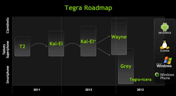
NVIDIA will eventually focus on improving per-core performance with subsequent iterations of the Tegra family (perhaps starting with Wayne in 2013), but until then Tegra 3 attempts to increase performance by exploiting thread level parallelism in Android.
GPU performance also sees a boon thanks to a larger and more efficient GPU in Tegra 3, but first let's talk about the CPU.
Tegra 3's Four Five Cores
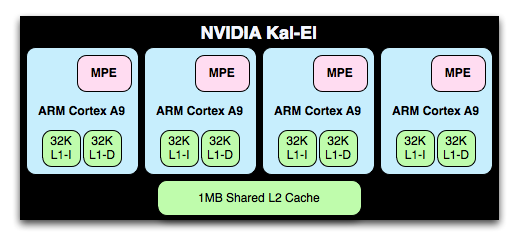
The Cortex A9 implementation in Tegra 3 is an improvement over Tegra 2; each core now includes full NEON support via an ARM MPE (Media Processing Engine). Tegra 2 lacked any support for NEON instructions in order to keep die size small.
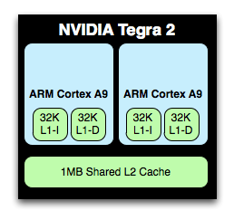
NVIDIA's Tegra 2 die
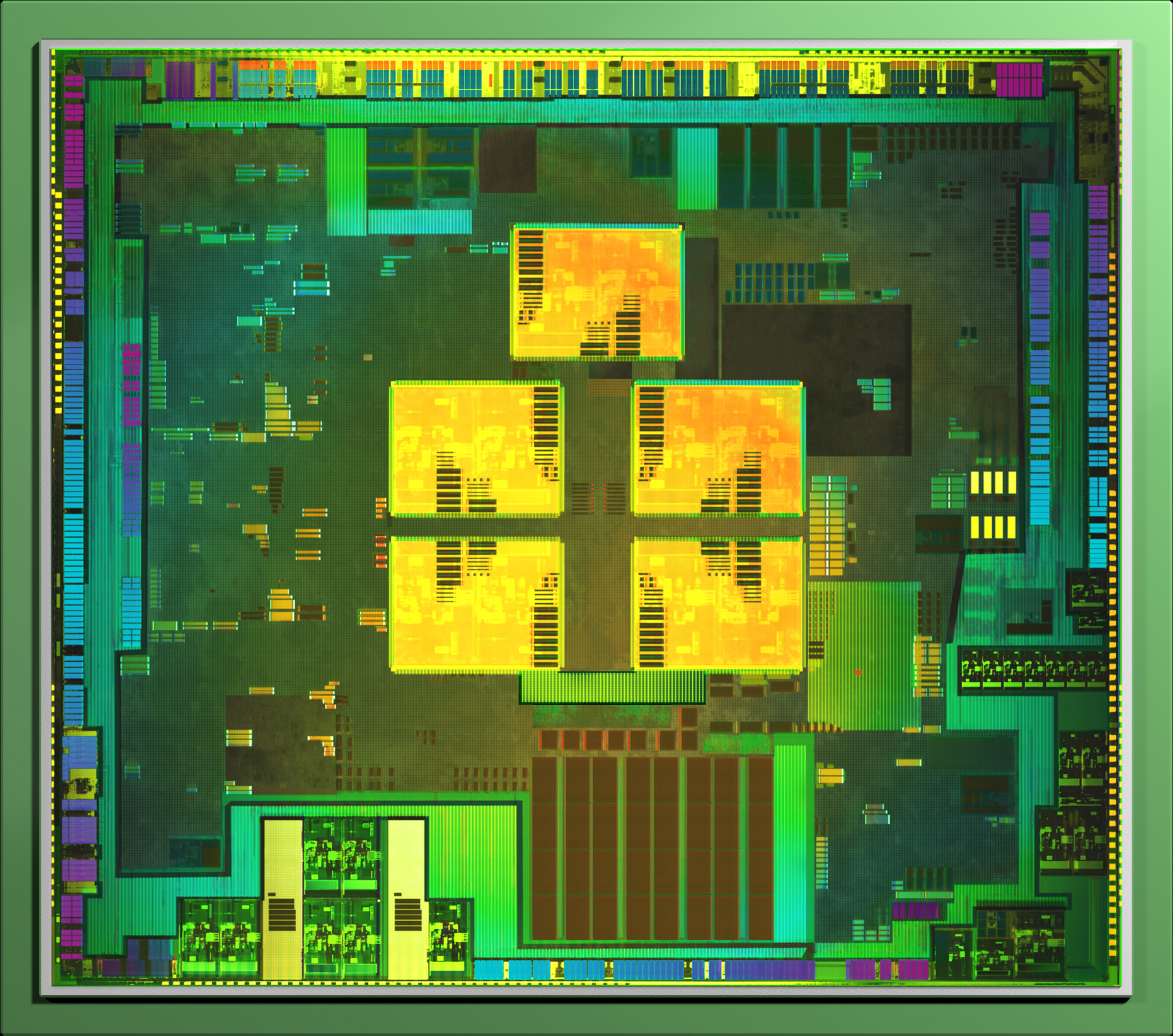
NVIDIA's Tegra 3 die, A9 cores highlighted in yellow
L1 and L2 cache sizes remain unchanged. Each core has a 32KB/32KB L1 and all four share a 1MB L2 cache. Doubling core count over Tegra 2 without a corresponding increase in L2 cache size is a bit troubling, but it does indicate that NVIDIA doesn't expect the majority of use cases to saturate all four cores. L2 cache latency is 2 cycles faster on Tegra 3 than 2, while L1 cache latencies haven't changed. NVIDIA isn't commenting on L2 frequencies at this point.
The A9s in Tegra 3 can run at a higher max frequency than those in Tegra 2. With 1 core active, the max clock is 1.4GHz (up from 1.0GHz in the original Tegra 2 SoC). With more than one core active however the max clock is 1.3GHz. Each core can be power gated in Tegra 3, which wasn't the case in Tegra 2. This should allow for lightly threaded workloads to execute on Tegra 3 in the same power envelope as Tegra 2. It's only in those applications that fully utilize more than two cores that you'll see Tegra 3 drawing more power than its predecessor.
The increase in clock speed and the integration of MPE should improve performance a bit over Tegra 2 based designs, but obviously the real hope for performance improvement comes from using four of Tegra 3's cores. Android is already well threaded so we should see gains in portions of things like web page rendering.
It's an interesting situation that NVIDIA finds itself in. Tegra 3 will show its biggest performance advantage in applications that can utilize all four cores, yet it will be most power efficient in applications that use as few cores as possible.
There's of course a fifth Cortex A9 on Tegra 3, limited to a maximum clock speed of 500MHz and built using LP transistors like the rest of the chip (and unlike the four-core A9 cluster). NVIDIA intends for this companion core to be used for the processing of background tasks, for example when your phone is locked and in your pocket. In light use cases where the companion core is active, the four high performance A9s will be power gated and overall power consumption should be tangibly lower than Tegra 2.
Despite Tegra 3 featuring a total of five Cortex A9 cores, only four can be active at one time. Furthermore, the companion core cannot be active alongside any of the high performance A9s. Either the companion core is enabled and the quad-core cluster disabled or the opposite.
NVIDIA handles all of the core juggling through its own firmware. Depending on the level of performance Android requests, NVIDIA will either enable the companion core or one or more of the four remaining A9s. The transition should be seamless to the OS and as all of the cores are equally capable, any apps you're running shouldn't know the difference between them.


94 Comments
View All Comments
jcompagner - Thursday, November 10, 2011 - link
does the OS not do the scheduling?I think there are loads of things build in to the OS that schedules the processors threads.. For example the OS must be Numa aware for numa systems so that they keep processes/threads on the right cores that are in the same cpu/memory banks
If i look at windows, then windows schedules everything all lover the place but it does now about hyper threading because those cores are skipped when i don't use more then 4 cores at the same time.
DesktopMan - Wednesday, November 9, 2011 - link
Seems risky to launch with a GPU that's weaker than existing SOCs. Compared to the Apple A5 performance it looks more like a 2009 product... Exynos also has it beat. The main competitor it beats is Qualcomm, who isn't far from launching new SOCs themselves.3DoubleD - Wednesday, November 9, 2011 - link
At least it looks more powerful than the SGX540 which is in the Galaxy Nexus. I'll wait and see what the real world performance is before writing it off. I suspect it will have "good enough" performance. I doubt we will see much improvement in Android devices until 28 nm as die sizes seem to be the limiting factor. Fortunately Nvidia has their name on the line here and they seem to be viciously optimizing their drivers to get every ounce of performance out of this thing.DesktopMan - Wednesday, November 9, 2011 - link
Totally agree on the Galaxy Nexus. That GPU is dinosaur old though. Very weird to use it in a phone with that display resolution. Any native 3d rendering will be very painful.eddman - Wednesday, November 9, 2011 - link
"Exynos also has it beat"We don't know that. On paper kal-el's geforce should be at least as fast as exynos. Better wait for benchmarks.
mythun.chandra - Wednesday, November 9, 2011 - link
It's all about the content. While it would be great to win GLBench and push out competition-winning benchmarks scores, what we've focused on is high quality content that fully exploits everything Tegra 3 has to offer.psychobriggsy - Friday, November 11, 2011 - link
I guess it depends on the clock speed the GPU is running at, and the efficiency it achieves when running. Whilst not as powerful per-clock (looking at the table in the article), a faster clock could make up a lot of the difference. Hopefully NVIDIA's experience with GPUs also means it is very efficient. Certainly the demos look impressive.But they're going to have to up their game soon considering the PowerVR Series 6, the ARM Mali 6xx series, and so on, as these are far more capable.
AmdInside - Wednesday, November 9, 2011 - link
Anyone else getting an error when opening the Asus Transformer Prime gallery?skydrome1 - Wednesday, November 9, 2011 - link
I am still quite underwhelmed by it's GPU. I mean, come on NVIDIA. A company with roots in GPU development having the lowest GPU performance?They need to up their game. Or everyone's just going to license other's IPs and develop their own SoCs. LG got an ARM license. Sony got an Imagination license. Samsung's even got their own SoCs shipping. Apple is sticking to in-house design. HTC acquired S3.
After telling the whole world that by the end of next year, there will be phones that will beat consoles in raw graphical performance, I feel like an idiot.
Please prove me right, NVIDIA.
EmaNymton - Wednesday, November 9, 2011 - link
REALLY getting tired of all the Anandtech articles being overly focused on performance and ignoring battery life or making statements about the technologies that will theoretically increase battery life. Total ACTUAL battery life matters and increases in perf shouldn't come to the detriment of total ACTUAL battery life.This over-emphasis on perf and refusing to hold MFGRs to account for battery life is bordering on irresponsible and is driving this behavior in the hardware MFGRs.
QUITE REWARDING THE HARDWARE MFGRs FOR RELEASING PRODUCTS WITH JUNK BATTERY LIFE OR BATTERY LIFE THAT IS WORSE THAN THE PREVIOUS GENERATION, ANANDTECH!