NVIDIA's Tegra 3 Launched: Architecture Revealed
by Anand Lal Shimpi on November 9, 2011 12:34 AM ESTASUS' Transformer Prime: The First Tegra 3 Tablet
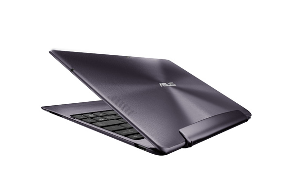
With Tegra 2, Motorola was the primary launch partner both for smartphones and tablets. Since then, ASUS has risen in the ranks and is now a serious competitor in the Android tablet space. It's no surprise that the first Tegra 3 tablet out of the gate is ASUS' Transformer Prime.

ASUS will launch the Transformer Prime in the US before the end of the year. The tablet's specs are below:
| Tablet Specification Comparison | ||||||
| ASUS Eee Pad Transformer | ASUS Eee Pad Transformer Prime | Apple iPad 2 | Samsung Galaxy Tab 10.1 | |||
| Dimensions | 271mm x 175mm x 12.95mm | 263 x 180.8 x 8.3mm | 241.2 x 185.7 x 8.8mm | 256.6 x 172.9 x 8.6mm | ||
| Display | 10.1-inch 1280 x 800 | 10.1-inch 1280 x 800 Super IPS+ | 9.7-inch 1024 x 768 IPS | 10.1-inch 1280 x 800 PLS | ||
| Weight | 675g | 586g | 601g | 565g | ||
| Processor | 1GHz NVIDIA Tegra 2 (2 x Cortex A9) | 1.3GHz NVIDIA Tegra 3 (4 x Cortex A9) | 1GHz Apple A5 (2 x Cortex A9) | 1GHz NVIDIA Tegra 2 (2 x Cortex A9) | ||
| Memory | 1GB | 1GB | 512MB | 1GB | ||
| Storage | 16GB + microSD card | 32GB/64GB + microSD slot | 16GB | 16GB | ||
| Pricing | $399 | $499/$599 | $499 | $499 | ||
Final Words
At a high level Tegra 3 doesn't surprise us much. The improved GeForce GPU should deliver tangible performance gains both through increased operating frequency and more pixel shader hardware. CPU performance should also be better than Tegra 2 based designs thanks to an increase in clock speed, the inclusion of MPE and the availability of more cores for threaded applications. In the move from one to two cores we saw significant performance increases across the board in Android. I don't expect that we'll see gains of a similar magnitude in moving from two to four cores, but there will be some benefit.
For the majority of use cases I believe NVIDIA has done the hardware homework necessary to extend battery life. Individual cores can now be power gated and the companion core should do most of the lifting while your device is locked or mostly idle, processing background tasks.
How much of an impact we'll actually see from all of this remains to be seen. We hope to have our hands on the first Tegra 3 hardware in the coming weeks, so before the year is up we'll hopefully have some answers.


94 Comments
View All Comments
dagamer34 - Wednesday, November 9, 2011 - link
Using 40nm isn't an excuse when both Apple and Samsung use 45nm and have GPUs that trounce the Tegra 2 in real life and Tegra 3 on paper.eddman - Wednesday, November 9, 2011 - link
Yeah, and A5 is about 42%-43% bigger than tegra 3, an seems to be consuming more power and run hotter. I'd rather have less GPU power than that.Don't know anything about exynos' size and other characteristics.
Anand, do you have any such information on exynos?
MySchizoBuddy - Wednesday, November 9, 2011 - link
what's your source of A5 die size?eddman - Wednesday, November 9, 2011 - link
At first this: http://www.anandtech.com/show/4840/kalel-has-five-...Anand says tegra 3 is 30% smaller than A5, which means A5 is 42-43% bigger.
After your above comment, I searched a little bit, and noticed in the IT pro portal article linked in my other comment, it says 120 mm^2.
I also found these:
http://www.eetimes.com/electronics-news/4215094/A5...
http://www.notebookcheck.net/Analyst-explains-grap...
Here, it's 122 mm^2.
Now with the exact size known, it puts the A5 in an even worse situation, 50-52% bigger.
eddman - Wednesday, November 9, 2011 - link
Ok, it seems exynos' size is about 118 mm^2.http://www.itproportal.com/2011/06/07/exynos-soc-s...
http://www.businesswire.com/news/home/201107070061...
Considering that tegra 3 has 5 cores and yet is still much smaller, I might say nvidia has actually done some nice engineering here.
Wonder how much of that difference is because of 40 nm process vs. 45 nm. Probably not much, but what do I know. Can anyone do some calculations?
metafor - Wednesday, November 9, 2011 - link
It's really difficult to judge because they're from two different foundries. The minimum etch (e.g. 45nm, 40nm) isn't the only thing that affects die area. Some processes require stricter design rules that end up bloating the size of logic.Samsung uses Samsung semi's foundries while nVidia uses TSMC. It's difficult to say how they compare without two identical designs that have gone to fab on both.
Klinky1984 - Wednesday, November 9, 2011 - link
I think the 500Mhz companion core & proper power gating alleviates most of the concerns about power consumption.metafor - Wednesday, November 9, 2011 - link
Not really. It alleviates the concern of power consumption on light loads. While that is a big part of common usage and it's definitely a benefit to have great idle/light power, I still would like to have better battery life while I'm heavily using the device. For instance, while playing a resource-heavy game or going to pretty complex websites.One thing I do like is that they've improved the efficiency of the video decoder. This makes one of the most common use-cases (watching movies) less power-intensive.
SniperWulf - Wednesday, November 9, 2011 - link
I agree. I would rather they had made a strong dual-core and dedicate the rest of the die space to a second memory channel and a stronger GPUa5cent - Wednesday, November 9, 2011 - link
Qualcom is the only SoC manufacturer making the transition to 28nm anytime soon. Everyone else is shifting at the very end of 2012 (at the earliest).