Understanding TLC NAND
by Kristian Vättö on February 23, 2012 1:14 PM EST- Posted in
- Storage
- SSDs
- OCZ
- Indilinx Everest
- TLC
Availability and Controller support
Just to make this clear, TLC isn't anything new. For example Hynix had a 32Gb 48nm TLC die in 2008. This is because TLC was originally used for devices like USB flash drives, where its poor endurance would be negligible. Most SSD OEMs have been toying with TLC SSDs for at least a year now but we haven't seen any commercial products. OCZ had originally planned to introduce its first TLC based SSD in the Q1 2012, however TLC pricing simply hasn't made sense yet. Unless OCZ can leverage a significant cost savings over 2-bit-per-cell MLC, the added headaches of bringing a lower performing TLC part to market don't make sense.
However there's still significant motivation to migrate towards TLC NAND. Further bringing down costs, particularly for consumer SSDs aimed at light, particularly read heavy workloads makes a lot of sense. Increasing pressure from Intel to deliver cheaper SSD enabled Ultrabooks, and Apple's desire to move all mainstream Macs to solid state storage are two major motivations. MLC NAND pricing will eventually get low enough to meet these (and more) needs, but TLC definitely accelerates the process.
TLC does require controller and firmware support. In the client SSD space only OCZ has been aggressive with announcing that its Indilinx Everest controller supports 3-bit-per-cell NAND.
Adding controller support for an extra bit per cell is more than just updating the datasheet and claiming it works. The ECC engine needs to be updated as the controller will face more frequent and more severe errors with TLC NAND (and its associated lower endurance rating).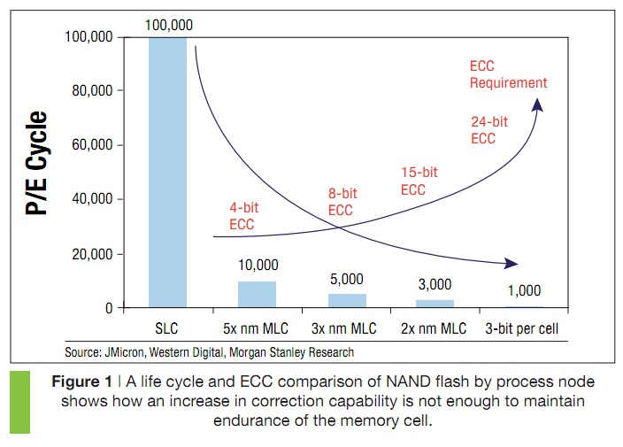
Maintaining low write amplification is even more important with TLC NAND. With significantly fewer available program/erase cycles, burning through them due to high write amplification isn't acceptible. While NAND endurance isn't really an issue for most client MLC drives, it may be an issue for TLC based drives.


90 Comments
View All Comments
Kougar - Thursday, February 23, 2012 - link
First, thanks for the article! However it has reignited a question I've had for some time.How is this regulated exactly... does the manufacturer still set a mandatory limit to the number or writes, or is a modern SSD capable of detecting this delay and automatically correcting for it up until the point that it is able to detect the block has exceeded the time limits (and hence write endurance) allowed? In another manner of phrasing it, are arbitrary write count limits utilized or is a modern SSD self-aware enough to determine on its own when a flash block needs to be retired, regardless of the write counts?
Kristian Vättö - Friday, February 24, 2012 - link
Each chip is slightly different so there is no set maximum of writes. One can last 3000 P/E cycles while the other can last 3200.I'm not 100% sure but I think the controller is the one who decides when a certain block is too slow. I.e. it's capable of detecting the delay and when it reaches a certain point, it decides to retire the block to avoid further performance decrease. Hence it may be controller specific and some will retire blocks sooner than others, although at least Intel is saying that there is a certain delay and after that the block is retired (but it may just be a recommendation).
Kougar - Friday, February 24, 2012 - link
Thank you for your reply, Kristian!When you mention every chip is different, that's a very excellent point and one of several reasons for the question.
The other reason behind my question was simply SSD lifespan... Anand has (several times) mentioned that even after the NAND "wears out" the data should remain readable for at least one year after that date.
Yet, all the SSD failures a huge number of others (including myself) have experienced has always been from an SSD suddenly failing outright, and not even being detected in the BIOS. I've yet to come across anyone that's claiming their drive became read only, or something else other than an outright failure or firmware related bug.Basically it seems like SSDs don't wear out, they just completely die outright for some reason. Going by your answer to my question, I'm going to safely assume NAND longevity isn't the factor in these episodes, but any input you may have on this would be quite welcome!
Kristian Vättö - Friday, February 24, 2012 - link
It's true that NAND remains readable when it wears out. For MLC, the period is about one year (eMLC is only 3 months, though).I can't say for sure what is the reason behind these early failures but I would claim that it's often controller related. In general, drives equipped with SandForce controllers experience more early failures than other drives (see the link below).
http://www.behardware.com/articles/843-7/component...
All the drives with +5% return rate are SandForce based, more specifically SF-1222 based. NewEgg yields similar data. SF-2281 based SSDs have quite a few one-star ratings, usually around 20%. Switch to Crucial or Intel (or any other non-SF drive) and we are looking at less than 10% one-star ratings, which usually imply a dead drive.
Of course, even non-SF drives experience early failures but the rate is much smaller and more common for consumer electronics. In any case, it's not the NAND that is causing the failure :-)
Sivar - Thursday, February 23, 2012 - link
I understand the necessity of reducing cost, but a sharp drop in durability coupled with a rapidly diminishing return on $savings/capacity due to the necessary greater redundancy seems a high price to pay for a linear increase in capacity.This is one of those articles that has the excellent writing and technical thoroughness characteristic of something written by Anand himself. To top it off, it doesn't use an inefficient image format for the photos with large areas of flat color, like the first image.
themossie - Friday, February 24, 2012 - link
Second that. Unusual clarity for any technical explanation. Thank you for the article, Kristian!hechacker1 - Friday, February 24, 2012 - link
I think the article got confusing by adding that that you can use less flash at 10.67Gb, along with 3bits per cell, giving 32Gb. Do the math: 10.67Gb * 3bits per cell = 32Gb.It's easier to just keep in mind:
16Gb NAND * 1 bit per cell = 16Gb capacity
16Gb NAND * 2 bit per cell = 32Gb capacity
16Gb NAND * 3 bit per cell = 48Gb capacity
Kristian Vättö - Friday, February 24, 2012 - link
The reason is that no final product has capacity of 48Gb. Capacities go in powers of 2: 2Gb, 4Gb, 8Gb, 16Gb, 32Gb, 64Gb and so on. 48Gb isn't a power of two (and no X*3 is). Hence you have to make the die smaller so that the X*3 is a power of two, like 10.67Gb is.In theory, you could make a 48Gb TLC die and it would work just fine. It's simply considered as an odd number in the NAND industry and hence not used.
themossie - Friday, February 24, 2012 - link
Kristian says this is awkward because TLC capacities will not scale from MLC capacities at a power of 2, like MLC did from SLC. I am not convinced that's an issue, as scaling capacity by a power of 2 has never been a requirement in the hard drive industry.Indeed, 80/90 GB SSDs - located between power-of-2-inspired 64 GB and 128 GB capacities - have been quite popular. For that matter, 64GB/128GB SSDs are often marketed as 60GB/120GB SSDs, partially due to provisioning...
It is awkward to describe 48Gb as 10.67Gb*3, where Gb represents physical transistors rather than bits; Gb is a unit for digital information in this context, not the physical representation of such.
This is exacerbated as the cells are physically identical - an array could store 48Gb using TLC, but only 10.67Gb with SLC. I find hechacker1's explanation more intuitive. 16Gb SLC = (16*2) 32Gb MLC = (16*3) 48Gb TLC...
The takeaway point here is that you get 50% more wafers per die for a given capacity with TLC over MLC, and this shows up directly in the cost ($0.60 cents/gb vs $0.90 cents/gb) but results in greatly reduced write cycles.
Kristian Vättö - Friday, February 24, 2012 - link
Remember that I'm not the one who came up with this idea ;-)This info is straight from Micron and they indeed say that the TLC die is chopped down to 10.67 billion transistors so that it becomes a 32Gb die. Maybe OEMs are afraid of adapting "odd number" capacities. In SSDs it wouldn't be so big deal but TLC is more commonly used in devices like USB flash drives and low-end smartphones. In fact, some OEMs may even use MLC and TLC in the same model (I don't have any examples but I wouldn't be surprised).
As for why some drives have an odd capacity, it has to do with the controller design and over-provisioning. Intel's SATA 3Gb/s controller has 10 channels while most controllers have 8. That's why Intel drives have weird capacities. Populate all 10 channels with 64Gb (8GB) dies and you get 80GB. For other drives, populating all the channels works out to be only 64GB. As for SandForce drives, they have no on-board cache (DRAM) so some of the NAND (~7%) is preserved for that. That's why 128GB SF drive is marketed as 120GB.
I agree that 10.67 is an awkward number but then again, this is stuff that an average consumer doesn't really need to know. For them, the final product will look the same, thanks to the power of two capacity. The gain of TLC is the same, no matter is the die smaller or the same as MLC. TLC provides more GB per die, which means cheaper $/GB.