ARM's Cortex A7: Bringing Cheaper Dual-Core & More Power Efficient High-End Devices
by Anand Lal Shimpi on October 19, 2011 12:31 PM EST- Posted in
- SoCs
- CPUs
- Arm
- Cortex A15
- Smartphones
- Mobile
- Cortex A7
- Tablets
big.LITTLE: Heterogeneous ARM MP
The Cortex A15 is going to be a significant step forward in performance for ARM architectures. ARM hopes it will be enough to actually begin to threaten the low end of the x86 space, which gives you an idea of just how powerful these cores are going to be. The A15 will also find its way into smartphones and tablets, ultimately replacing the Cortex A9s used by high-end devices today.
For heavy workloads, the Cortex A15 is expected to be more power efficient than the A9. The core may draw more instantaneous power, but it will do so for a shorter period of time thus allowing the CPU(s) to get to sleep quicker and reducing average power.
As ARM has often argued (particularly against Intel) however, these big out-of-order microprocessor architectures are inefficient at dealing with lightweight mobile workloads. In particular, things like background tasks running on your phone while it’s locked in your pocket simply don’t demand the performance of a Cortex A15. ARM further argues that the power consumed by an A15 running these tasks, even though only for a short period of time, is greater than it would be on a much simpler in-order architecture. This is where the A7 comes into play.
Although the Cortex A7 is fully capable of being used on its own (and it most definitely will be), ARM’s partners are free to integrate Cortex A7 cores alongside Cortex A15 cores in a big.LITTLE (or little.BIG?) configuration.
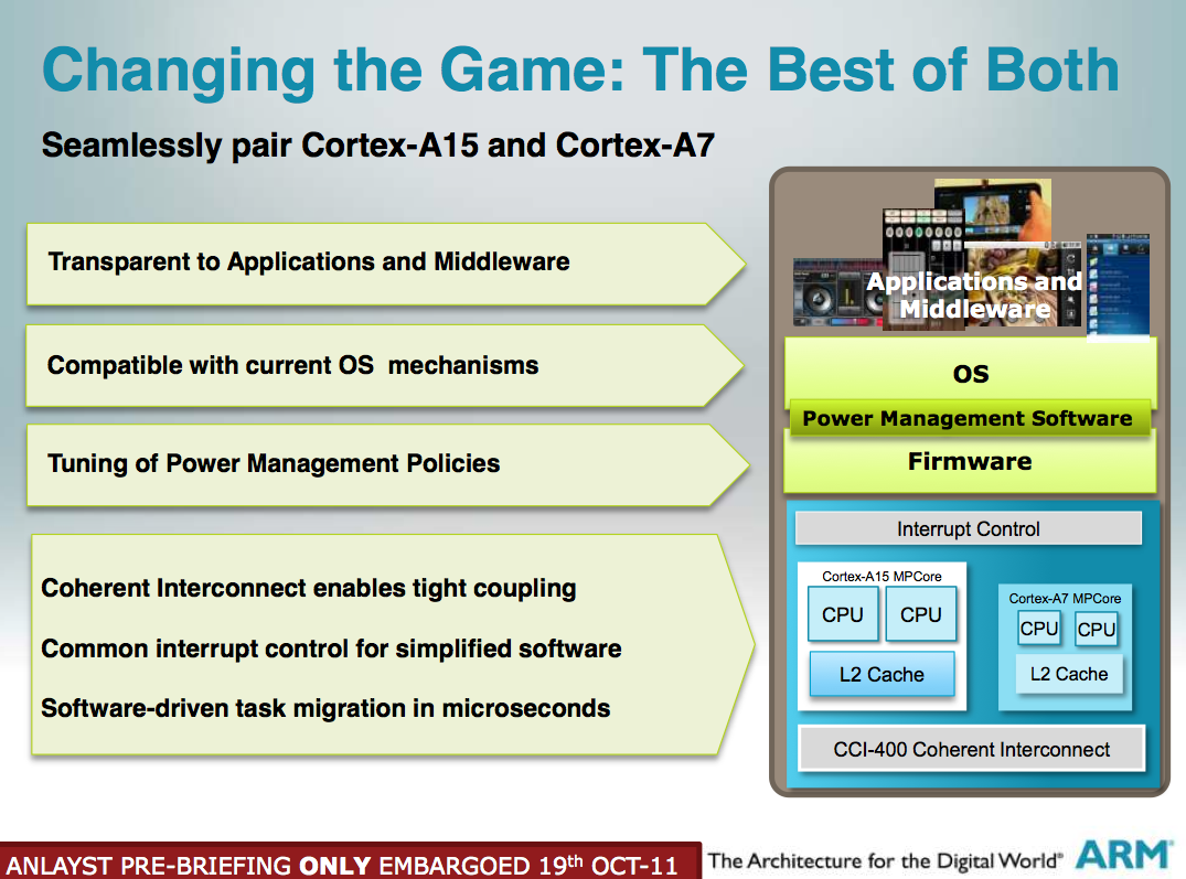
Since the A7 and A15 are equally capable of executing the same ARM instruction set, any applications running on one core can just as easily be migrated to run on the other. In the example above there are a pair of A15s and a pair of A7s on a single SoC. In this particular configuration, the OS only believes there are two cores in the machine. ARM’s own power management firmware determines which core cluster to activate depending on performance states requested by the OS. If the OS wants a high performance state, ARM returns the A15 cores at a high p-state. If it wants a low performance state, the chip will put the A15s to sleep and schedule everything on the A7s. Cache coherency is guaranteed via the CCI-400 interconnect, so any data invalidated by one core cluster will be reflected in the other cluster’s cache. ARM claims it can switch between core clusters in this configuration in as quick as 20 microseconds.
If everything works the way ARM has described it, a big.LITTLE configuration should be perfectly transparent to the OS (similar to what NVIDIA is promising with Kal-el). ARM did add that SoC vendors are free to expose all cores to the OS if they would like, although doing so would obviously require OS awareness of the different core types.
Core Configurations, Process Technology & Final Words
ARM’s Cortex A7 will be available in 1 - 4 core configurations, both as the primary CPU in an SoC as well as in a big.LITTLE configuration alongside some A15s. ARM expects that we will see some 40nm A7 designs as early as the end of next year for use in low end smartphones (~$100). Most smartphone configurations, even at these price points will likely use dual-core A7 implementations. It’s only in emerging markets that ARM is expecting to see single core Cortex A7 smartphone devices. This is pretty big news as it means that even value smartphones will be dual-core by 2013.
Costs will keep the A7 on 40nm for a while although the cores will be offered at 28nm for integration into A15 designs as well as for even higher performance/lower power implementations.
I have to say that I’m pretty excited about the Cortex A7 announcement across the board. It looks like this core will not only enable much better performance at the value end of the device spectrum but it should bring battery life improvements at the high end as well. Chip architects have argued for years that we were going to see heterogeneous computing as the next phase in the evolution of microprocessors, it’s fascinating to see that we may get the first consumer application of it in ultra mobile devices.


75 Comments
View All Comments
Manabu - Saturday, October 22, 2011 - link
The decode portion of the chip also have to grow if one wants higher IPC/power efficiency. So it is probably more than 0.3% nowadays.fic2 - Wednesday, October 19, 2011 - link
The problem with Atom power wise was Intel stupidly decided to saddle it with a chipset that was 3 (?) fab generations behind (Atom: 45nm, chipset: 130nm) and used more power than the actual cpu. I don't know if they have corrected this part of the problem but it seems to be an Intel trait - get most of it right but screw up on the last mile thing. (Compare that to AMD that either gets it right (Zacate, Llano) or gets it very wrong (Bulldozer) or ARM which seems to get a most everything right).fteoath64 - Thursday, October 20, 2011 - link
Good point. Chipset development has been a secondary priority for Intel, this way they ensure the combo solution is good-enough for the market to make the volumes they intended. Looking into the past when other chipset makers like Nvidia, AMD and SiS, even VIA at some stage did a better chipset implementation than Intel.Atom was not aggressive enough to leverage low-power and has little integration of other SoC components like most of the chipset features. At least most of the north/south bridges leaving only external I/O interfaces. A lousy slow GPU is their burden, so plenty of legacy not solved.
Intel had better be careful because ARM A15 has the capability to upset X86 in future by software emulation with multicore heterogeneous chips.
fteoath64 - Thursday, October 20, 2011 - link
Well said. Atom has already sunk, just that Intel is in denial mode. I was suggesting that Intel swallows their pride and GET an Arm license so they can design and manufacture these chips and compete with Qualcomm and Samsung in the ARM market. At least it will give them some volume game instead of having zero in mobile.If they continue with Atom architecture, they will learn a costly mistake later on. This way they can evolve a single core SB low power and maybe a bare-bones atom core small.BIG evolution. It could just secures their Win8 tablets for X86 (if that market ever develops...).
B3an - Wednesday, October 19, 2011 - link
A GPU is not a CPU. And intel have more than once before that they are NOT capable of matching ARM. And i dont expect them to for a long time, if ever.Wolfpup - Wednesday, October 19, 2011 - link
Yeah, I was thinking "hey, Intel could stick an Atom on a better chip" before he said that.This IS very interesting (as is what Nvidia is doing even before this), but it's interesting because it's an interesting idea...I don't see how it effects Intel one way or the other. Obviously if other companies can do it, Intel can do it too.
JPForums - Thursday, October 20, 2011 - link
<quote>It's this kind of heterogeneous SoC structure with different CPU architectures on a single die that will nail Intel to the wall and prevent them from ever really penetrating the mobile market. </quote>The idea of heterogeneous architectures isn't new. ARM is simply applying them differently. IBM's cell processor (used in the PS3) uses a combination of general purpose processing core(s) and specialized lighter weight cores. Quite a while back Intel's vision of the future involved processors with a combination of a few complex heavy weight cores and many lightweight cores (think Larrabee or similar). With power saving features largely complete and an upcoming GPU that is supposed to be competitive I wouldn't be surprised if Intel started to get more serious about bringing this to market. They have already made great strives with their tera-scale research: 48 core single chip, 80 core research chip.
What ARM did that was innovative, was to use a heterogeneous architecture for the purposes of power savings, and to make it appear homogenous. I would argue that with Intel's focus on power gating and other power saving features, the idea of using a heterogeneous architecture to save power hasn't escaped them. However, full instruction set compatibility between the two architectures makes things much simpler as the different cores remain largely transparent to the OS and applications. While it isn't really that hard to develop separate code paths to use more efficient instructions when available, this does raise the complexity on the OS for thread scheduling. Hiding these cores is mostly a convenience, though. It puts the burden of moving to a lower power core largely on the chip and again reduces the complexity of the thread scheduler.
A more effective use of heterogeneous architectures would be to reveal the presence of all cores to the OS and to individually power gate them. (Individual power states would be even better.) This would allow the use of lower power cores any time for threads that don't require higher performance. I.E. two high performance apps and low OS background tasks would take place on two A15 cores and an A7 rather than three A15s. Further, once the OS starts intelligently assigning tasks to processors, it can become advantageous to have slight differences in the architectures of some cores to support specific tasks.
I see this move as a necessary one to get OS makers and app developers thinking along the lines of heterogeneous processing while providing a progressive move over path. Intel's I64 architecture failed largely due to the fact that it forced a clean break from past applications. AMD's A64 architecture succeeded because people didn't have to leave behind old applications and code going forward (at least no until they were ready to). That said, I don't think ARM intends to stop here long term. While a cell like approach with significantly different cores would be less than optimal, smaller differences like the lack of full NEON or SSE4 support on lower power cores shouldn't be much of a burden once the OS/apps are smart enough to route threads to a core with the necessary units available.
MJEvans - Wednesday, October 19, 2011 - link
This is exactly the kind of competition that the market has needed. AMD used to be able to keep up to Intel's heals with intelligent decisions and hand-tuning to make the most of being on a mature process node as opposed to a cutting/bleeding edge one. ARM's decisions here represent the logic of applying that at a macroscopic (architectural) level.Arnulf - Wednesday, October 19, 2011 - link
I was contemplating this few months ago before Kal-El was described in media and existence of its extra core revealed to public. Something along the lines of 2x Atom + 2x Sandy Bridge cores, with all cores visible to the OS.OS should be able to identify each core and allocate the workload to it accordingly - i.e. OS would grab one of the weaker cores for itself, schedule CPU intensive processes on more powerful cores and have one low-power core in reserve just in case (for antivirus etc.).
This would result in CPUs with maximum TDP only ~5-10W above existing models yet it would allow for far less conext switching. There is no point in hiding those weaker cores from the OS; instead OS should be intelligent enough to to utilize them to the fullest extent.
psychobriggsy - Thursday, October 20, 2011 - link
For seamless *running* application migration between the different core types, they should both support the exact same instruction set extensions, which currently Atom and SB don't. I don't think that AMD's Bobcat and Bulldozer do either.I wouldn't say no to a chip comprising of a Bulldozer module or two (like Trinity), and a couple of Bobcat cores as well for lower-power modes. This would surely save a lot of power over even Bulldozer in its lowest operational clock/power state.
However neither AMD nor Intel can compete in power against this ARM technology - A15 for power (around Bobcat performance per core) and A7 for power saving (around 1GHz Atom performance per core I would imagine). As soon as Intel takes a step towards lower power with Atom, ARM moves the goalposts. Even an Atom core implemented at 22nm can't compete with a 28nm 0.5mm^2 core... which is practically free in terms of silicon (even with a small L2 cache added on top).