ARM's Cortex A7: Bringing Cheaper Dual-Core & More Power Efficient High-End Devices
by Anand Lal Shimpi on October 19, 2011 12:31 PM EST- Posted in
- SoCs
- CPUs
- Arm
- Cortex A15
- Smartphones
- Mobile
- Cortex A7
- Tablets
big.LITTLE: Heterogeneous ARM MP
The Cortex A15 is going to be a significant step forward in performance for ARM architectures. ARM hopes it will be enough to actually begin to threaten the low end of the x86 space, which gives you an idea of just how powerful these cores are going to be. The A15 will also find its way into smartphones and tablets, ultimately replacing the Cortex A9s used by high-end devices today.
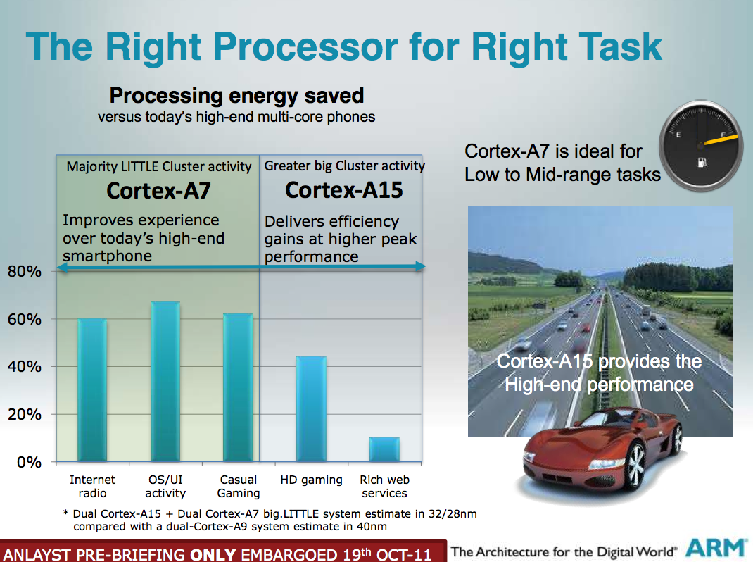
For heavy workloads, the Cortex A15 is expected to be more power efficient than the A9. The core may draw more instantaneous power, but it will do so for a shorter period of time thus allowing the CPU(s) to get to sleep quicker and reducing average power.
As ARM has often argued (particularly against Intel) however, these big out-of-order microprocessor architectures are inefficient at dealing with lightweight mobile workloads. In particular, things like background tasks running on your phone while it’s locked in your pocket simply don’t demand the performance of a Cortex A15. ARM further argues that the power consumed by an A15 running these tasks, even though only for a short period of time, is greater than it would be on a much simpler in-order architecture. This is where the A7 comes into play.
Although the Cortex A7 is fully capable of being used on its own (and it most definitely will be), ARM’s partners are free to integrate Cortex A7 cores alongside Cortex A15 cores in a big.LITTLE (or little.BIG?) configuration.
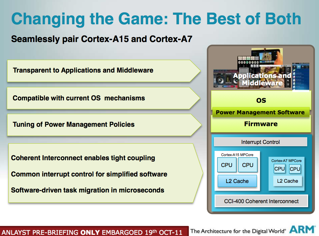
Since the A7 and A15 are equally capable of executing the same ARM instruction set, any applications running on one core can just as easily be migrated to run on the other. In the example above there are a pair of A15s and a pair of A7s on a single SoC. In this particular configuration, the OS only believes there are two cores in the machine. ARM’s own power management firmware determines which core cluster to activate depending on performance states requested by the OS. If the OS wants a high performance state, ARM returns the A15 cores at a high p-state. If it wants a low performance state, the chip will put the A15s to sleep and schedule everything on the A7s. Cache coherency is guaranteed via the CCI-400 interconnect, so any data invalidated by one core cluster will be reflected in the other cluster’s cache. ARM claims it can switch between core clusters in this configuration in as quick as 20 microseconds.
If everything works the way ARM has described it, a big.LITTLE configuration should be perfectly transparent to the OS (similar to what NVIDIA is promising with Kal-el). ARM did add that SoC vendors are free to expose all cores to the OS if they would like, although doing so would obviously require OS awareness of the different core types.
Core Configurations, Process Technology & Final Words
ARM’s Cortex A7 will be available in 1 - 4 core configurations, both as the primary CPU in an SoC as well as in a big.LITTLE configuration alongside some A15s. ARM expects that we will see some 40nm A7 designs as early as the end of next year for use in low end smartphones (~$100). Most smartphone configurations, even at these price points will likely use dual-core A7 implementations. It’s only in emerging markets that ARM is expecting to see single core Cortex A7 smartphone devices. This is pretty big news as it means that even value smartphones will be dual-core by 2013.
Costs will keep the A7 on 40nm for a while although the cores will be offered at 28nm for integration into A15 designs as well as for even higher performance/lower power implementations.
I have to say that I’m pretty excited about the Cortex A7 announcement across the board. It looks like this core will not only enable much better performance at the value end of the device spectrum but it should bring battery life improvements at the high end as well. Chip architects have argued for years that we were going to see heterogeneous computing as the next phase in the evolution of microprocessors, it’s fascinating to see that we may get the first consumer application of it in ultra mobile devices.


75 Comments
View All Comments
dagamer34 - Wednesday, October 19, 2011 - link
It's this kind of heterogeneous SoC structure with different CPU architectures on a single die that will nail Intel to the wall and prevent them from ever really penetrating the mobile market.A5 - Wednesday, October 19, 2011 - link
Intel is perfectly capable of doing the same thing, so I'm not sure why you say that. They do it now in a different direction with the on-die SB GPU...metafor - Wednesday, October 19, 2011 - link
They won't be able to implement a small, energy-efficient processor similar to Kingfisher (Cortex A7). While at performance/complexity levels of A15, the x86 decode penalty is relatively small, as you get down to ~100mW levels at the die area we're talking about, there simply isn't an x86 core out there that is feasible.jeremyshaw - Wednesday, October 19, 2011 - link
Intel already has the CE4100, a SoC designed for TVs. It just isn't a main point they are focusing on right now, as they are competing against IBM RISC (some 200W per CPU is possible on those :eek:), while having to scale all the way down. Intel even has to focus on IGP, wireless, ethernet, etc. Intel is doing the best they can against an overwheling slew of competitors at all angles in all directions. However, I do not have doubts in their ability to compete when why need to. Right now, they have some big fish to fry (IBM), and it's not like Intel hasn't made ARM chips before (XScale).Not to mention... they still hold their traditional fab advantage over everyone else.
But do I think Intel may lose out if they don't start making some serious pushes into the smartphone SoC market? Yes, I do. However, Google/Intel have already anounced all future versions of Android will be officiall support x86, in addition to ARM. This works for existing Android apps, too, due to the JIT nature of Android apps (Dalvik).
jeremyshaw - Wednesday, October 19, 2011 - link
the next time I post on a tablet... I won't, lol.name99 - Wednesday, October 19, 2011 - link
"Intel is doing the best they can against an overwheling slew of competitors at all angles in all directions."Actually Intel has made the deliberate decision that FULL x86 compatibility trumps everything else. This saddles Atom with a huge amount of basically useless baggage that ARM is not carrying. This baggage takes up space, uses power, and, most importantly, makes it that much more difficult to execute and validate a chip fast.
This is not "doing the best they can". It is a stupid, short-sighted decision made by execs who have drunk their own koolaid and can't imagine that some decisions made by Intel in the 1980s may not be optimal for today. Atom SHOULD have been a stripped down x86-64 CPU with EVERYTHING not essential to that mission jettisoned. One (modern) way of doing everything and the rest --- 286 mode, V x86 mode, PAE, SMM, x87, MMX etc etc tossed overboard. But that ship has sailed. Intel have made their bed, and now they will have to lie in it --- the same mindset that sank iTanic will sink Atom in its target market.
Guspaz - Wednesday, October 19, 2011 - link
x86 compatibility is not a significant burden on modern chips; transistor density is increasing far faster than the number of x86 instructions is, and Intel's chips have been effectively RISC since the Pentium Pro, when they started translating x86 into micro-ops internally. CISC on the outside, RISC on the inside.In 2008, when Anand wrote his Atom architecture article (http://www.anandtech.com/show/2493/3), he pointed out AMD had told him that x86 decoding consumed only 10% of the transistor count of the K8, and current transistor densities are ~35x higher than they were then (130nm -> 22nm).
By that math, that means that x86 decoding consumes only about 0.3% of a modern desktop processor, almost inconsequential.
metafor - Wednesday, October 19, 2011 - link
It is not a significant burden on modern large chips. The type of profile that the Cortex A7 fits in (~0.5mm^2) will see a large burden from x86 decoding.On a desktop or even low-profile laptop chip, x86 compatibility doesn't cost much. On a tiny CPU meant to only process a smartphone's background processes, it can cost a lot.
name99 - Wednesday, October 19, 2011 - link
Allow me to explain how English works to you. You see this statement "and, most importantly, makes it that much more difficult to execute and validate a chip fast."?That means if you wish to refute my point, you have to attack the claim that I said was MOST IMPORTANT.
Do you deny that Intel has an insanely complex task designing and validating their chips, vastly more so than ARM? Do you deny that the major reason for that complexity is all the x86 baggage?
iwod - Thursday, October 20, 2011 - link
Like i wrote below, Atom and SandyBridge are different thing. Atom does not support SSE 4, Some Do not support Hyper Threading, Some dont have Intel 64, and it also lacks the new SandyBridge AVX.I am not expert, but since Intel Atom and SB will have different Micro-Op Cache, Unless you write your software on the lowest common denominator, which is the Atom. You cant have the software works the same way as ARM has currently show with A7 and A9.
Yes, with some software tricks and profile i suppose the problem isn't Very hard to tackle. But in terms of software development ARM should be much easier.