Intel's Ivy Bridge Architecture Exposed
by Anand Lal Shimpi on September 17, 2011 2:00 AM EST- Posted in
- CPUs
- Intel
- Ivy Bridge
- IDF 2011
- Trade Shows
The New GPU
Westmere marked a change in the way Intel approached integrated graphics. The GPU was moved onto the CPU package and used an n-1 manufacturing process (45nm when the CPU was 32nm). Performance improved but it still wasn't exactly what we'd call acceptable.
Sandy Bridge brought a completely redesigned GPU core onto the processor die itself. As a co-resident of the CPU, the GPU was treated as somewhat of an equal - both processors were built on the same 32nm process.
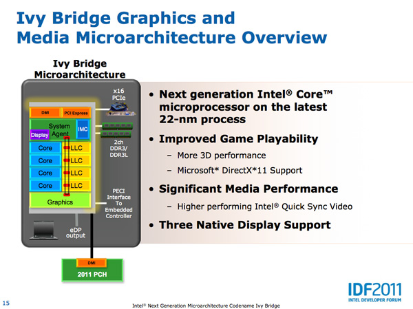
With Ivy Bridge the GPU remains on die but it grows more than the CPU does this generation. Intel isn't disclosing the die split but there are more execution units this round (16 up from 12 in SNB) so it would appear as if the GPU occupies a greater percentage of the die than it did last generation. It's not near a 50/50 split yet, but it's continued indication that Intel is taking GPU performance seriously.
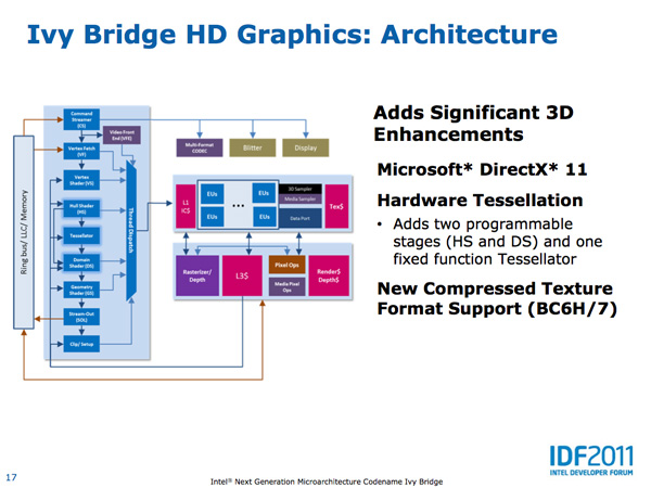
The Ivy Bridge GPU adds support for OpenCL 1.1, DirectX 11 and OpenGL 3.1. This will finally bring Intel's GPU feature set on par with AMD's. Ivy also adds three display outputs (up from two in Sandy Bridge). Finally, Ivy Bridge improves anisotropic filtering quality. As Intel Fellow Tom Piazza put it, "we now draw circles instead of flower petals" referring to image output from the famous AF tester.
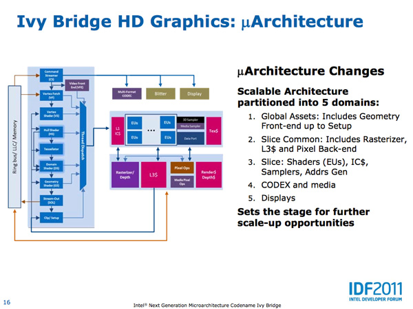
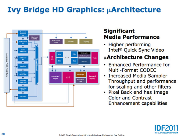
Intel made the Ivy Bridge GPU more modular than before. In SNB there were two GPU configurations: GT1 and GT2. Sandy Bridge's GT1 had 6 EUs (shaders/cores/execution units) while GT2 had 12 EUs, both configurations had one texture sampler. Ivy Bridge was designed to scale up and down more easily. GT2 has 16 EUs and 2 texture samplers, while GT1 has an unknown number of EUs (I'd assume 8) and 1 texture sampler.
I mentioned that Ivy Bridge was designed to scale up, unfortunately that upwards scaling won't be happening in IVB - GT2 will be the fastest configuration available. The implication is that Intel had plans for IVB with a beefier GPU but it didn't make the cut. Perhaps we will see that change in Haswell.
As we've already mentioned, Intel is increasing the number of EUs in Ivy Bridge however these EUs are much better performers than their predecessors. Sandy Bridge's EUs could co-issue MADs and transcendental operations, Ivy Bridge can do twice as many MADs per clock. As a result, a single Ivy Bridge EU gets close to twice the IPC of a Sandy Bridge EU - in other words, you're looking at nearly 2x the GFLOPS in shader bound operations as Sandy Bridge per EU. Combine that with more EUs in Ivy Bridge and this is where the bulk of the up-to-60% increase in GPU performance comes from.
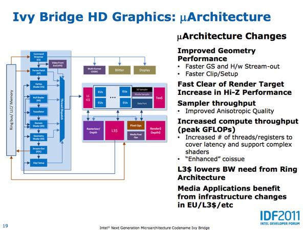
Intel also added a graphics-specific L3 cache within Ivy Bridge. Despite being able to share the CPU's L3 cache, a smaller cache located within the graphics core allows frequently accessed data to be accessed without firing up the ring bus.
There are other performance enhancements within the shader core. Scatter & gather operations now execute 32x faster than Sandy Bridge, which has implications for both GPU compute and general 3D gaming performance.
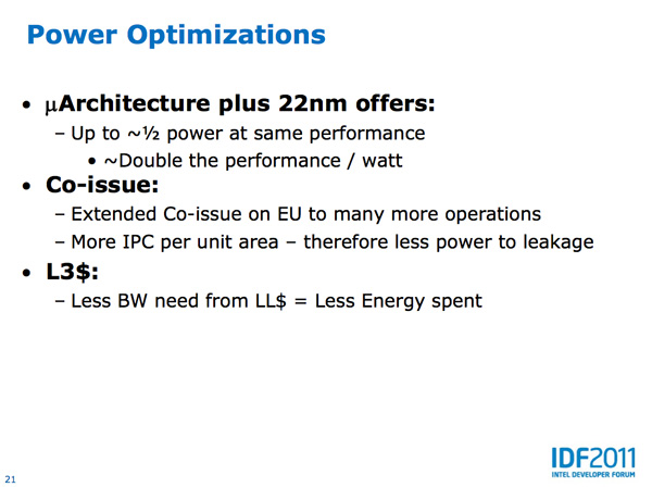
Despite the focus on performance, Intel actually reduced the GPU clock in Ivy Bridge. It now runs at up to 95% of the SNB GPU clock, at a lower voltage, while offering much higher performance. Thanks primarily to Intel's 22nm process (the aforementioned architectural improvements help as well), GPU performance per watt nearly doubles over Sandy Bridge. In our Llano review we found that AMD delivered much longer battery life in games (nearly 2x SNB) - Ivy Bridge should be able to help address this.


Quick Sync Performance Improved
With Sandy Bridge Intel introduced an extremely high performing hardware video transcode engine called Quick Sync. The solution ended up delivering the best combination of image quality and performance of any available hardware accelerated transcoding options from AMD, Intel and NVIDIA. Quick Sync leverages a combination of fixed function hardware, IVB's video decode engine and the EU array.
The increase in EUs and improvements to their throughput both contribute to increases in Quick Sync transcoding performance. Presumably Intel has also done some work on the decode side as well, which is actually one of the reasons Sandy Bridge was so fast at transcoding video. The combination of all of this results in up to 2x the video transcoding performance of Sandy Bridge. There's also the option of seeing less of a performance increase but delivering better image quality.
I've complained in the past about the lack of free transcoding applications (e.g. Handbrake, x264) that support Quick Sync. I suspect things will be better upon Ivy Bridge's arrival.


97 Comments
View All Comments
driscoll42 - Saturday, September 17, 2011 - link
On the last page there's "Should the fab engineers at Intel do their job well, Ivy Bridge could deliver much better power characteristics than Ivy." in the second paragraph, should that be Sandy on the end?Anand Lal Shimpi - Saturday, September 17, 2011 - link
Thank you! Fixed :)Take care,
Anand
Beenthere - Saturday, September 17, 2011 - link
It's good that Intel has decided that their GPU sucks and that to be competitive they need to catch up to AMD. This will take some time as AMD has a two year head start on APUs but it's all good for consumers.In spite of the marketing hype from Intel it looks like they've conceded that AMD has the better system approach with APUs for mainstream consumers and laptops. CPU performance alone is no longer a valid yardstick for PC performance thanks to AMD's advance thinking and Llano.
TypeS - Saturday, September 17, 2011 - link
I realize Intel is behind (has been for since anyone can remember) in the graphics arena compared to AMD/ATI and NVIDIA, but is AMD "two years ahead" in terms of an APU? While Clarkdale can't really be considered a true all in one package (hey remember when Kentsfield wasn't considered a true quad core?), it was still an all in one package, and with Sandy Bridge, Intel brought it all together onto one die. Intel isn't calling it an APU but if you compare SNB and Llano/Bulldozer, they share some similarities.AMD's edge is on graphics, and Intel is closing the gap.
I might be missing something though in why you say they are ahead in terms of an "APU", but from my knowledge, Intel as first to release a retail/commercial APU.
Guspaz - Monday, September 19, 2011 - link
Intel might be catching up in terms of physical performance, but Intel's drivers still, quite frankly, suck. It's the one thing really holding the platform back, in terms of both compatibility and performance. Even simple things like flash acceleration can sometimes be wonky with Intel's drivers.Furthermore, developers like Carmack have been pestering Intel to give them lower-level access to the hardware, with potentially enormous performance benefits; they'd like to treat PCs more like a console, and stripping away much of the driver/graphics overhead (particularly in terms of memory management) could see some pretty big performance gains. There's a reason why modern integrated GPUs like in Ivy Bridge have theoretical performance on-par with a 360 or PS3, but in practice, are nowhere near as performant.
Of course, the same is true for AMD and nVidia; high-end developers like Carmack and Sweeney seem to want lower-level access to hardware. From Carmack's latest QuakeCon keynote, it does seem like the hardware manufacturers are listening.
fic2 - Monday, September 19, 2011 - link
Yeah, Intel seems to want to catch up and made a pretty decent effort of no sucking with the HD3000. BUT then they go and do a dumb@ss thing like put the crappy HD2000 on 90% of the Sandies they sell. I think if marketing would get the he11 out of the way they wouldn't be too sucky.Oh, yeah, except the drivers.
bigboxes - Saturday, September 17, 2011 - link
I love AMD as much as the next guy (have three running AMD boxes), but are you going to continue to be "that guy" that posts this nonsense in every Intel/AMD thread? We get it. You love AMD and want to help them win the CPU wars. Yay for fanbois everywhere!Beenthere - Saturday, September 17, 2011 - link
Intel hasn't released an APU. They have released a CPU and GPU on the same slab of silicon. That's not an integrated APU.No nonsense, just facts. I like facts. Some folks can't handle facts but that's life. I like choice and scrupulous businesses. That's what AMD is unlike Intel.
ltcommanderdata - Saturday, September 17, 2011 - link
For someone arguing against marketing hype and looking for facts you seem overly preoccupied by AMD's APU term. If you are looking for which product currently on the market has tighter CPU/IGP integration then that produce is Sandy Bridge not Llano. For instance Sandy Bridge allows bidirectional communication/sharing of instructions and data between the CPUs and IGP via a shared on die L3 cache instead of through a crossbar and off die system memory as in Llano. Sandy Bridge also has more advanced power and thermal monitoring allowing efficient sharing of TDP room between the CPU and IGP, allowing each to be overclocked as needed, something Llano doesn't do.Yes, Llano has the faster GPU, but that's not the critical concern if what you are interested in is integration. Intel's CPU and GPU on a slab of silicon was Arrandale. Sandy Bridge has moved well beyond that. Llano's CPU/GPU integration looks to be somewhere in between Arrandale and Sandy Bridge. Seeing Llano is AMD's 1st generation Fusion product along with Brazos that's fine. But just because AMD's calls their product an APU doesn't mean it's the pinnacle of CPU/GPU integration.
gramboh - Sunday, September 18, 2011 - link
Boom. Beenthere just got roasted, and of course disappears rather than admitting he was wrong.