Desktop Llano Motherboards: The ASRock A75 Extreme6 Preview
by Ian Cutress on June 14, 2011 12:00 AM EST- Posted in
- Motherboards
- ASRock
- Llano
The motherboard currently on the test bed is a pre-production model provided to us by ASRock, so I must stress that the design is not completely finalised. As far as I'm aware, the heatsink design isn't finished, nor the extras in retail package or the BIOS. I'm currently running a BIOS which requires some work to get finished, , hence I'm holding out for the retail product for a full review. But the board layout is done:
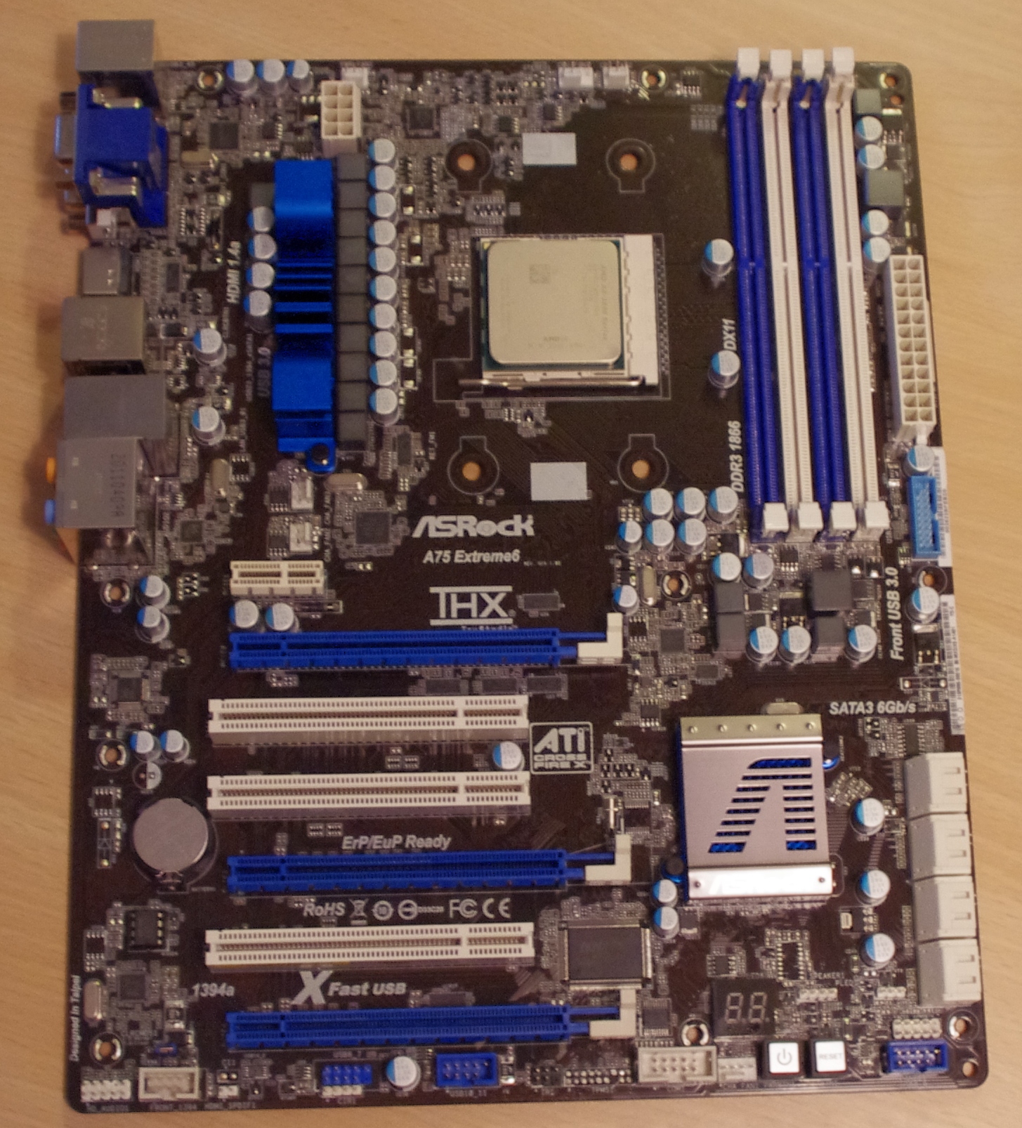
What we have is a fairly regular board with very few surprises. The AMD FM1 socket takes up a lot of space, and the 8+2 phase, without its final heatsink design, doesn't encroach on the socket area. There are plenty of fan headers around the socket—two for the CPU (one four-pin), one SYS and two chassis headers. This is a nice number of headers around the socket, as long as the software is there to control the chassis and CPU ones.
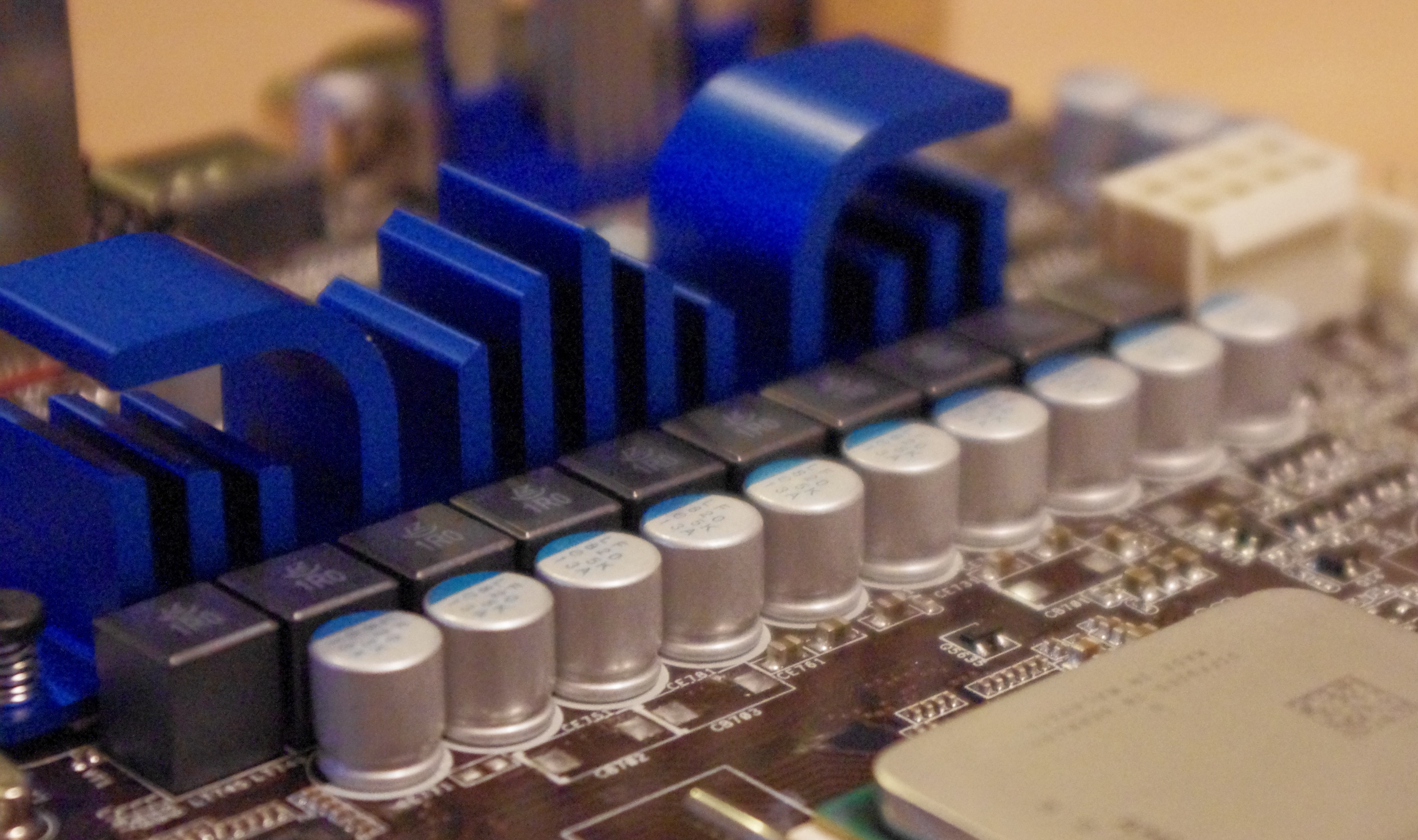
The four DIMM slots support DDR3-1866, and are located by an onboard USB 3.0 header. Underneath this are eight SATA 6 Gbps ports—six from the Fusion Controller Hub, and one from a controller. The usual ASRock Power/Reset and Debug LED combination is here (it is the Extreme6, we'd expect it to be), as well as two USB 2.0 headers, a COM header and a Firewire header. The FCH is tucked away under a small ASRock heatsink.

The PCIe layout makes full use of the three PCI that the A75/Hudson-D3 supports—by having three PCIe x16 and one PCe x1 at the top. The top two PCIe x16 are split x16/x0 or x8/x8, the bottom one is linked x4 via the UMI, but its throughput will be determined on what else is in use through the FCH. No doubt the lack of more PCIe x1 may be an issue for some.
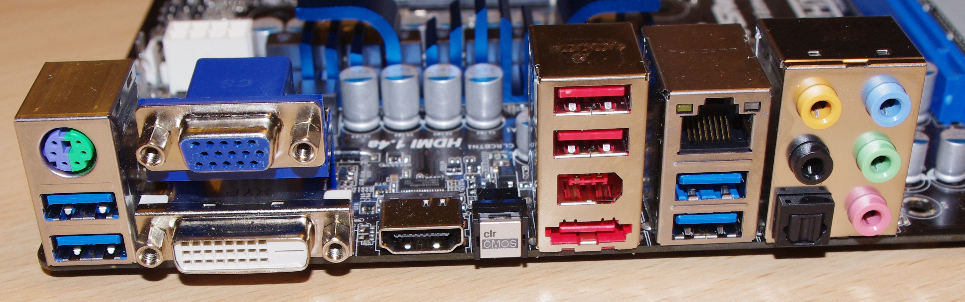
The IO panel has some issues. There is a large gap above the HDMI port which with the right setup could have a couple more USB ports, but the biggest one by far is the DVI display port. With a cable in here, I had trouble getting any USB product, apart from a nano-USB stick, into the USB ports to the left—including my USB mouse and keyboard. It's a tight fit, and this oversight is courtesy of a lack of testing. Altogether, there's four USB 3.0 ports on the back, two USB 2.0 ports, a gigabit Ethernet port, a clear CMOS button, a Firewire port, an eSATA port and standard array of audio connectors.


BIOS and Overclocking
The BIOS on the ASRock board is similar to what we've seen in previous ASRock motherboards on the Sandy Bridge platform. As the board is not ready for release yet, it's still very rough around the edges. For now, it has a lot of options you wouldn't see, particularly in the RAM timing section, or the overclocking options.
What we can tell you right now is that overclocking is limited to the bus speed. This is confirmed by ASRock—even if the BIOS allows you to set a multiplier, this isn't actually implemented in the OS. Even if it's set at 36x, it'll still be 29x in reality. This means that there's little credence into many of the overclocked results you may have seen online—the only way to clock the processor is bus speed only. It starts at 100 MHz, and it's a case of raising and testing stability. With some minor testing, I hit 115 MHz quite easily (29*115 = 3.33 GHz), but I have a feeling it's going to be very dependent on the processor and motherboard.


43 Comments
View All Comments
marc1000 - Tuesday, June 14, 2011 - link
Ian, I believe that in the "release to market" boards, the memory speed should be configured according to the official maximum speed of each platform. if that means 1333 for intel and 1800 (or whatever the final spec may be) for AMD, then this is the way it should be tested. maybe AMD was aiming for higher speed to compensate for the low number of channels. ;)KaarlisK - Tuesday, June 14, 2011 - link
Seconded.If a platform supports DDR3-1866, it is an actual advantage of the platform and it should be used.
There is the question of cost, though.
IanCutress - Tuesday, June 14, 2011 - link
Noted for the future. It's always interesting to hear what other people think on the issue.Ian
semo - Tuesday, June 14, 2011 - link
Do AMD motherboards fully support UEFI like this ASRock?mino - Thursday, June 16, 2011 - link
UEFI support is PURELY motherboard vendor's choice.It has nothing to do with the CPU, be it AMD, Intel or VIA for that matter.
mino - Thursday, June 16, 2011 - link
Err, better wording would be "has UEFI", as the board either uses UEFI or BIOS loader.It does not "support" either. It contains/uses them.
DanNeely - Tuesday, June 14, 2011 - link
How many PCIe lanes does the southbridge have in total? If it's low enough (eg the same 4 as the mobile part + 4 on the CPU), then the 3 legacy PCI slots might simply reflect not being able to add anything else?The ethernet and additional sata controllers would take two; and if the firewire controller is PCIe instead of PCI that would take a 3rd, leaving only the 5 used in the 1x and 3rd 16x(phy) slot.
Alternately, are they using AMD audio or a 3rd party controller? The latter would take a connection as well.
mino - Thursday, June 16, 2011 - link
Exactly.glugglug - Tuesday, June 14, 2011 - link
Is there an AMD equivalent of QuickSync? To me, that is the biggest plus of SandyBridge right now.Shinobi_III - Tuesday, June 14, 2011 - link
I hope there's some sort of safety here, resetting that would suck while running..