The OCZ Vertex 3 Review (120GB)
by Anand Lal Shimpi on April 6, 2011 6:32 PM ESTOverall System Performance using PCMark Vantage
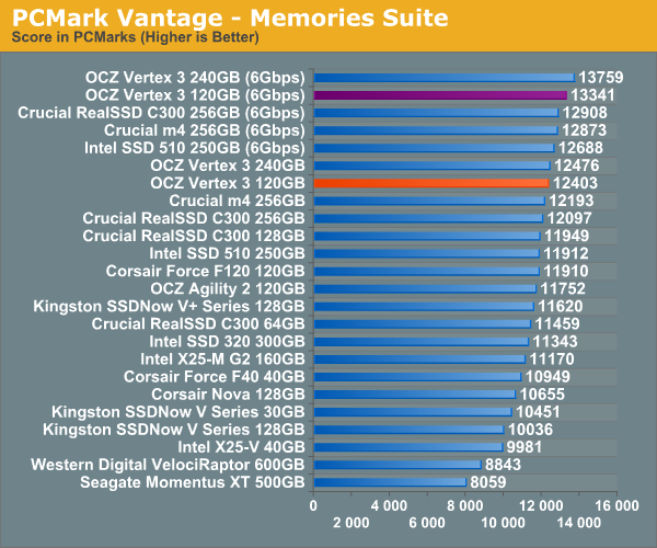
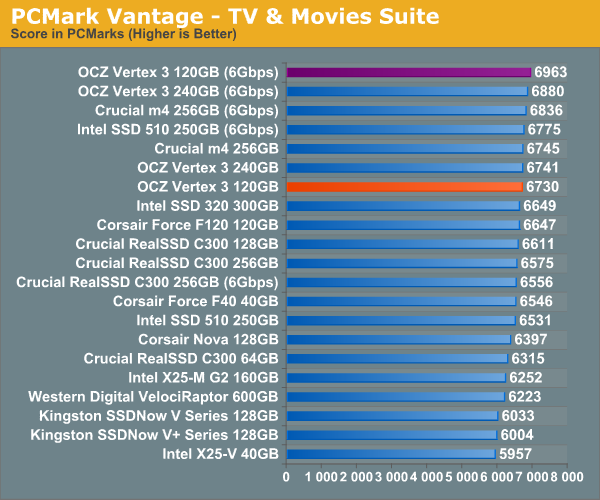
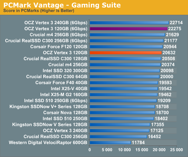
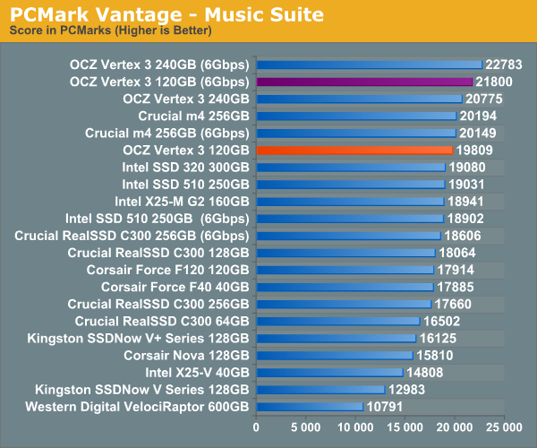
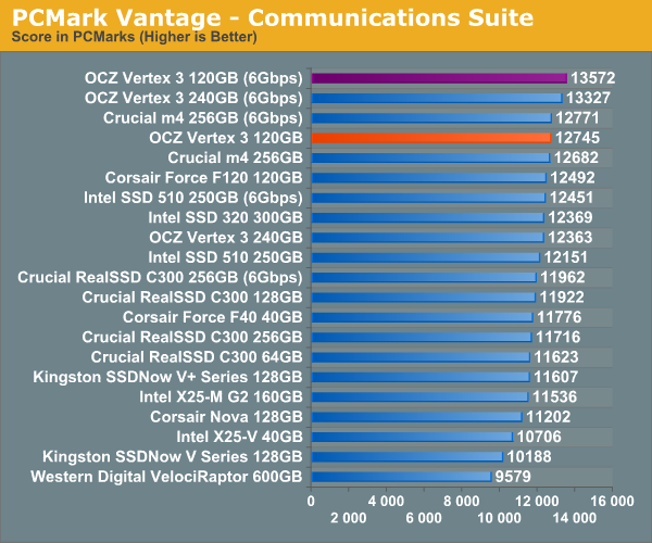
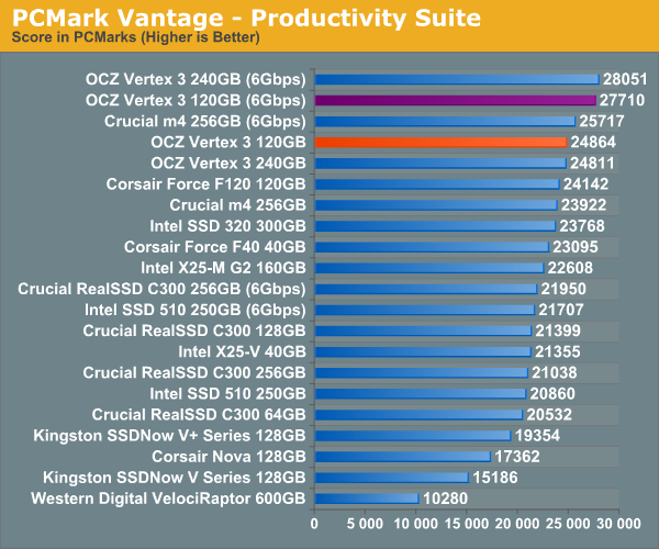
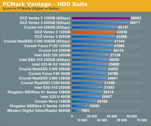
Next up is PCMark Vantage, another system-wide performance suite. For those of you who aren’t familiar with PCMark Vantage, it ends up being the most real-world-like hard drive test I can come up with. It runs things like application launches, file searches, web browsing, contacts searching, video playback, photo editing and other completely mundane but real-world tasks. I’ve described the benchmark in great detail before but if you’d like to read up on what it does in particular, take a look at Futuremark’s whitepaper on the benchmark; it’s not perfect, but it’s good enough to be a member of a comprehensive storage benchmark suite. Any performance impacts here would most likely be reflected in the real world.
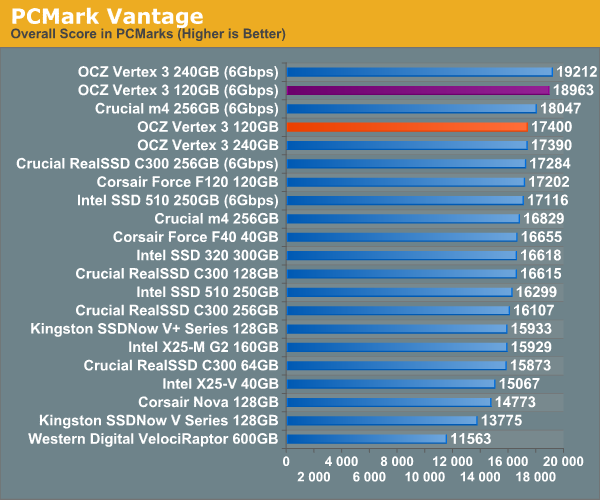
If we use PCMark as an indication of light system performance, the Vertex 3 120GB does pretty well here.


153 Comments
View All Comments
dagamer34 - Wednesday, April 6, 2011 - link
Any idea when these are going to ship out into the wild? I've got a 120GB Vertex 2 in my 2011 MacBook Pro that I'd love to stick into my Windows 7 HTPC so it's more responsive.Ethaniel - Wednesday, April 6, 2011 - link
I just love how Anand puts OCZ on the grill here. It seems they'll just have to step it up. I was expecting some huge numbers coming from the Vertex 3. So far, meh.softdrinkviking - Wednesday, April 6, 2011 - link
"OCZ insists that there's no difference between the Spectek stuff and standard Micron 25nm NAND"Except for the fact that Spectek is 34nm I am assuming?
There surely must be some significant difference in performance between 25 and 34, right?
softdrinkviking - Wednesday, April 6, 2011 - link
sorry, i think that wasn't clear.what i mean is that it seems like you are saying the difference in process nodes is purely related to capacity, but isn't there some performance advantage to going lower as well?
softdrinkviking - Wednesday, April 6, 2011 - link
okay. forget it. i looked back through and found the part where you write about the 25nm being slower.that's weird and backwards. i wonder why it gets slower as it get smaller, when cpus are supposedly going to get faster as the process gets smaller?
are their any semiconductor engineers reading this article who know?
are the fabs making some obvious choice which trades in performance at a reduced node for cost benefits, in an attempt to increase die capacities and lower end-user costs?
lunan - Thursday, April 7, 2011 - link
i think because the chip get larger but IO interface to the controller remain the same (the inner raid). instead of addressing 4GB of NAND, now one block may consists of 8GB or 16GB NAND.in case of 8 interface,
4x8GB =32GB NAND but 8x8GB=64GB NAND, 8x16GB=128GB NAND
the smaller the shrink is, the bigger the nand, but i think they still have 8 IO interface to the controller, hence the time takes also increased with every shrinkage.
CPU or GPU is quite different because they implement different IO controller. the base architecture actually changes to accommodate process shrink.
they should change the base architecture with every NAND if they wish to archive the same speed throughput, or add a second controller....
I think....i may not be right >_<
lunan - Thursday, April 7, 2011 - link
for example the vertex 3 have 8GB NAND with 16(8 front and 8 back) connection to the controller. now imagine if the NAND is 16GB or 32 GB and the interface is only 16 with 1 controller?maybe the CPU approach can be done to this problem. if you wish to duplicate performace and storage, you do dual core (which is 1 cpu core beside the other)....
again...maybe....
softdrinkviking - Friday, April 8, 2011 - link
thanks for your reply. when i read it, i didn't realize that those figures were referring to the capacity of the die.as soon as i re-read it, i also had the same reaction about redesigning the controller, it seems the obvious thing to do,
so i can't believe that the controller manufacturer's haven't thought of it.
there must be something holding them back, probably $$.
the major SSD players all appear to be trying to pull down the costs of drives to encourage widespread adoption.
perhaps this is being done at the expense of obvious performance increases?
Ammaross - Thursday, April 7, 2011 - link
I think if you re-reread (yes, twice), you'll note that with the die shrink, the block size was upped from 4K to 8K. This is twice the space to be programmed or erased per write. This is where the speed performance disappears, regardless of the number of dies in the drive.Anand Lal Shimpi - Wednesday, April 6, 2011 - link
Sorry I meant Micron 34nm NAND. Corrected :)Take care,
Anand