NVIDIA's GeForce GTX 550 Ti: Coming Up Short At $150
by Ryan Smith on March 15, 2011 9:00 AM ESTGTX 550 Ti’s Quirk: 1GB Of VRAM On A 192-bit Bus
One thing that has always set NVIDIA apart from AMD is their willingness to use non-power of 2 memory bus sizes. AMD always sticks to 256/128/64 bit busses, while NVIDA has used those along with interesting combinations such as 384, 320, and 192 bit busses. This can allow NVIDIA to tap more memory bandwidth by having a wider bus, however they also usually run their memory slower than AMD’s memory on comparable products, so NVIDIA’s memory bandwidth advantage isn’t quite as pronounced. The more immediate ramifications of this however are that NVIDIA ends up with equally odd memory sizes: 1536MB, 1280MB, and 768MB.
768MB in particular can be problematic. When the GTX 460 launched, NVIDIA went with two flavors: 1GB and 768MB, the difference being how many memory controller/ROP blocks were enabled, which in turn changed how much RAM was connected. 768MB just isn’t very big these days – it’s only as big as NVIDIA’s top of the line card back at the end of 2006. At high resolutions with anti-aliasing and high quality textures it’s easy to swamp a card, making 1GB the preferred size for practically everything from $250 down. So when NVIDIA has a 768MB card and AMD has a 1GB card, NVIDIA has a definite marketing problem and a potential performance problem.
| Video Card Bus Width Comparison | ||||||||
| NVIDIA | Bus Width | AMD | Bus Width | |||||
| GTX 570 | 320-bit | Radeon HD 6970 | 256-bit | |||||
| GTX 560 Ti | 256-bit | Radeon HD 6950 | 256-bit | |||||
| GTX 460 768MB | 192-bit | Radeon HD 6850 | 256-bit | |||||
| GTX 550 Ti | 192-bit | Radeon HD 5770 | 128-bit | |||||
| GTS 450 | 128-bit | Radeon HD 5750 | 128-bit | |||||
NVIDIA’s solution is to normally outfit cards with more RAM to make up for the wider bus, which is why we’ve seen 1536MB and 1280MB cards going against 1GB AMD cards. With cheaper cards though the extra memory (or higher density memory) is an extra cost that cuts in to margins. So what do you do when you have an oddly sized 192-bit memory bus on a midrange card? For GTS 450 NVIDIA disabled a memory controller to bring it down to 128-bit, however for GTX 550 Ti they needed to do something different if they wanted to have a 192-bit bus while avoiding having only 768MB of memory or driving up costs by using 1536MB of memory. NVIDIA’s solution was to put 1GB on a 192-bit card anyhow, and this is the GTX 550 Ti’s defining feature from a technical perspective.
Under ideal circumstances when inter leaving memory banks you want the banks to be of equal capacity, this allows you to distribute most memory operations equally among all banks throughout the entire memory space. Video cards with their non-removable memory have done this for ages, however full computers with their replaceable DIMMs have had to work with other layouts. Thus computers have supported additional interleaving options beyond symmetrical interleaving, most notably “flex” interleaving where one bank is larger than the other.
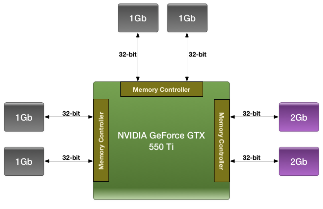
It’s this technique that NVIDIA has adopted for the GTX 550 Ti. GF116 has 3 64-bit memory controllers, each of which is attached to a pair of GDDR5 chips running in 32bit mode. All told this is a 6 chip configuration, with NVIDIA using 4 1Gb chips and 2 2Gb chips. In the case of our Zotac card – and presumably all GTX 550 Ti cards – the memory is laid out as illustrated above, with the 1Gb devices split among 2 of the memory controllers, while both 2Gb devices are on the 3rd memory controller.
This marks the first time we’ve seen such a memory configuration on a video card, and as such raises a number of questions. Our primary concern at this point in time is performance, as it’s mathematically impossible to organize the memory in such a way that the card always has access to its full theoretical memory bandwidth. The best case scenario is always going to be that the entire 192-bit bus is in use, giving the card 98.5GB/sec of memory bandwidth (192bit * 4104MHz / 8), meanwhile the worst case scenario is that only 1 64-bit memory controller is in use, reducing memory bandwidth to a much more modest 32.8GB/sec.
How NVIDIA spreads out memory accesses will have a great deal of impact on when we hit these scenarios, and at this time they are labeling the internal details of their memory bus a competitive advantage, meaning they’re unwilling to share the details of its operation with us. Thus we’re largely dealing with a black box here, which we’re going to have to poke and prod at to try to determine how NVIDIA is distributing memory operations.
Our base assumption is that NVIDIA is using a memory interleaving mode similar to “flex” modes on desktop computers, which means lower memory addresses are mapped across all 3 memory controllers, while higher addresses are mapped to the remaining RAM capacity on the 3rd memory controller. As such NVIDIA would have the full 98.5GB/sec of memory bandwidth available across the first 768MB, while the last 256MB would be much more painful at 32.8GB/sec. This isn’t the only way to distribute memory operations however, and indeed NVIDIA doesn’t have to use 1 method at a time thanks to the 3 memory controllers, so the truth is likely much more complex.
Given the black box nature of GTX 550’s memory access methods, we decided to poke at things in the most practical manner available: CUDA. GPGPU operation makes it easy to write algorithms that test the memory across the entire address space, which in theory would make it easy to determine GTX 550’s actual memory bandwidth, and if it was consistent across the entire address space. Furthermore we have another very similar NVIDIA card with a 192-bit memory bus on hand – GTX 460 768MB – so it would be easy to compare the two and see how a pure 192-bit card would compare.
We ran in to one roadblock however: apparently no one told the CUDA group that GTX 550 was going to use mixed density memory. As it stands CUDA (and other APIs built upon it such as OpenCL and DirectCompute) can only see 768MB minus whatever memory is already in use. While this lends support to our theory that NVIDIA is using flex mode interleaving, this makes it nearly impossible to test the theory at this time as graphics operations aren’t nearly as flexible enough (and much more prone to caching) to test this.
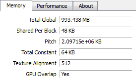
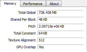
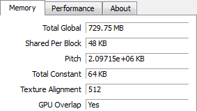
CUDA-Z: CUDA Available Memory. Clockwise, Top-Left: GTS 450, GTX 460 768MB, GTX 550 Ti
At this point NVIDIA tells us it’s a bug and that it should be fixed by the end of the month, however until such a time we’re left with our share of doubts. Although this doesn’t lead to any kind of faulty operation, this is a pretty big bug to slip through NVIDIA’s QA process, which makes it all the more surprising.
In the meantime we did do some testing against the more limited memory capacity of the GTX 550. At this point the results are inconclusive at best. Using NVIDIA’s Bandwidth Test CUDA sample program, which is a simple test to measure memcopy bandwidth of the GPU, we tested the GTS 450, GTX 468 768MB, GTX 460 1GB, and GTX 550 Ti at both stock and normalized (GTX 460) clocks. The results were inconclusive – the test seems to scale with core clocks far more than memory bandwidth – which may be another bug, or an artifact of the program having originally been written pre-Fermi. In any case here is the data, but we have low confidence in it.
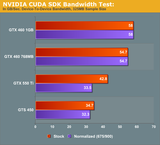
As it stands the test shows almost no gain over the GTS 450 at normalized clocks; this doesn’t make a great deal of sense under any memory interleaving scheme, hence the low confidence. If and when all the bugs that may be causing this are fixed, we’ll definitely be revisiting the issue to try to better pin down how NVIDIA is doing memory interleaving.


79 Comments
View All Comments
Ryan Smith - Tuesday, March 15, 2011 - link
Our experience with desktop Linux articles in the past couple of years is that there's little interest from a readership perspective. The kind of video cards we normally review are for gaming purposes, which is lacking to say the least on Linux. We could certainly try to integrate Linux in to primary GPU reviews, but would it be worth the time and what we would have to give up in return? Probably not. But if you think otherwise I'm all ears.HangFire - Tuesday, March 15, 2011 - link
All I'm asking for is current and projected CUDA/OpenCL level support, and what OS distro's and revisions are supported.You may not realize it, but all this GPGPU stuff is really used in science, government and defense work. Developers often get the latest and greatest gaming card and when it is time for deployment, middle end cards (like this one) are purchased en masse.
Nividia and AMD have been crowing about CUDA and OpenCL, and then deliver spotty driver coverage for new and previous generation cards. If they are going to market it heavily, they should cough up the support information with each card release, we shouldn't have to call the corporate rep and harangue them each and every time.
Belard - Wednesday, March 16, 2011 - link
Someone who already has a GF450 would be a sucker to spend $150 for a "small-boost" upgraded card.When upgrading, a person should get a 50% or better video card. A phrase that never applies to a video card is "invest" since they ALL devalue to almost nothing. Todays $400~500 cards are tomorrows $150 cards and next weeks $50.
So a current GF450 owner should look at a GF570 or ATI 6900 series cards for a good noticeable bump.
mapesdhs - Wednesday, March 16, 2011 - link
Or, as I've posted before, a 2nd card for SLI/CF, assuming their mbd
and the card supports it. Whether or not this is worthwhile and the
issues which affect the outcome is what I've been researching in recent
weeks. Sorry I can't post links due to forum policy, but see my earlier
longer post for refs.
Ian.
HangFire - Friday, March 18, 2011 - link
I wasn't really suggesting such an upgrade (sidegrade). I was just saying that each generation card at a price point and naming convention (450->550) should have at least a little better performance than card it replaces.Calabros - Tuesday, March 15, 2011 - link
tell me a reason to NOT prefer 6850 over this7Enigma - Tuesday, March 15, 2011 - link
So basically this is my 4870 in a slightly lower power envelope with DX11 features. I'm shocked the performance is so low honestly. Thanks for including the older cards in the review because it's always nice to see I'm still chugging along just fine at my gaming resolution (1280X1024) 19".7Enigma - Tuesday, March 15, 2011 - link
Forgot to add, which I bought in Jan 2009 for $180 (Sapphire Toxic 512meg VaporX, so not reference design)mapesdhs - Tuesday, March 15, 2011 - link
You're the target audience for the work I've been doing, comparing cards at
that kind of resolution, old vs. new, and especially where one is playing older
games, etc. Google for, "Ian PC Benchmarks", click the 1st result, then select,
"PC Benchmarks, Advice and Information". I hope to be able to obtain a couple
of 4870s or 4890s soon, though there's already a lot of 4890 results included.
Ian.
morphologia - Tuesday, March 15, 2011 - link
Why in the name of all that's graphical would you use this Noah's Ark menagerie of cards but leave out the 4890? It doesn't make sense. If you're going to include 4000 series cards, you must include the top-of-the-line single-GPU card. It's proven to be quite competitive even now, against the lower-level new cards.