NVIDIA's GeForce GTX 550 Ti: Coming Up Short At $150
by Ryan Smith on March 15, 2011 9:00 AM ESTGTX 550 Ti’s Quirk: 1GB Of VRAM On A 192-bit Bus
One thing that has always set NVIDIA apart from AMD is their willingness to use non-power of 2 memory bus sizes. AMD always sticks to 256/128/64 bit busses, while NVIDA has used those along with interesting combinations such as 384, 320, and 192 bit busses. This can allow NVIDIA to tap more memory bandwidth by having a wider bus, however they also usually run their memory slower than AMD’s memory on comparable products, so NVIDIA’s memory bandwidth advantage isn’t quite as pronounced. The more immediate ramifications of this however are that NVIDIA ends up with equally odd memory sizes: 1536MB, 1280MB, and 768MB.
768MB in particular can be problematic. When the GTX 460 launched, NVIDIA went with two flavors: 1GB and 768MB, the difference being how many memory controller/ROP blocks were enabled, which in turn changed how much RAM was connected. 768MB just isn’t very big these days – it’s only as big as NVIDIA’s top of the line card back at the end of 2006. At high resolutions with anti-aliasing and high quality textures it’s easy to swamp a card, making 1GB the preferred size for practically everything from $250 down. So when NVIDIA has a 768MB card and AMD has a 1GB card, NVIDIA has a definite marketing problem and a potential performance problem.
| Video Card Bus Width Comparison | ||||||||
| NVIDIA | Bus Width | AMD | Bus Width | |||||
| GTX 570 | 320-bit | Radeon HD 6970 | 256-bit | |||||
| GTX 560 Ti | 256-bit | Radeon HD 6950 | 256-bit | |||||
| GTX 460 768MB | 192-bit | Radeon HD 6850 | 256-bit | |||||
| GTX 550 Ti | 192-bit | Radeon HD 5770 | 128-bit | |||||
| GTS 450 | 128-bit | Radeon HD 5750 | 128-bit | |||||
NVIDIA’s solution is to normally outfit cards with more RAM to make up for the wider bus, which is why we’ve seen 1536MB and 1280MB cards going against 1GB AMD cards. With cheaper cards though the extra memory (or higher density memory) is an extra cost that cuts in to margins. So what do you do when you have an oddly sized 192-bit memory bus on a midrange card? For GTS 450 NVIDIA disabled a memory controller to bring it down to 128-bit, however for GTX 550 Ti they needed to do something different if they wanted to have a 192-bit bus while avoiding having only 768MB of memory or driving up costs by using 1536MB of memory. NVIDIA’s solution was to put 1GB on a 192-bit card anyhow, and this is the GTX 550 Ti’s defining feature from a technical perspective.
Under ideal circumstances when inter leaving memory banks you want the banks to be of equal capacity, this allows you to distribute most memory operations equally among all banks throughout the entire memory space. Video cards with their non-removable memory have done this for ages, however full computers with their replaceable DIMMs have had to work with other layouts. Thus computers have supported additional interleaving options beyond symmetrical interleaving, most notably “flex” interleaving where one bank is larger than the other.
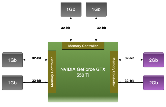
It’s this technique that NVIDIA has adopted for the GTX 550 Ti. GF116 has 3 64-bit memory controllers, each of which is attached to a pair of GDDR5 chips running in 32bit mode. All told this is a 6 chip configuration, with NVIDIA using 4 1Gb chips and 2 2Gb chips. In the case of our Zotac card – and presumably all GTX 550 Ti cards – the memory is laid out as illustrated above, with the 1Gb devices split among 2 of the memory controllers, while both 2Gb devices are on the 3rd memory controller.
This marks the first time we’ve seen such a memory configuration on a video card, and as such raises a number of questions. Our primary concern at this point in time is performance, as it’s mathematically impossible to organize the memory in such a way that the card always has access to its full theoretical memory bandwidth. The best case scenario is always going to be that the entire 192-bit bus is in use, giving the card 98.5GB/sec of memory bandwidth (192bit * 4104MHz / 8), meanwhile the worst case scenario is that only 1 64-bit memory controller is in use, reducing memory bandwidth to a much more modest 32.8GB/sec.
How NVIDIA spreads out memory accesses will have a great deal of impact on when we hit these scenarios, and at this time they are labeling the internal details of their memory bus a competitive advantage, meaning they’re unwilling to share the details of its operation with us. Thus we’re largely dealing with a black box here, which we’re going to have to poke and prod at to try to determine how NVIDIA is distributing memory operations.
Our base assumption is that NVIDIA is using a memory interleaving mode similar to “flex” modes on desktop computers, which means lower memory addresses are mapped across all 3 memory controllers, while higher addresses are mapped to the remaining RAM capacity on the 3rd memory controller. As such NVIDIA would have the full 98.5GB/sec of memory bandwidth available across the first 768MB, while the last 256MB would be much more painful at 32.8GB/sec. This isn’t the only way to distribute memory operations however, and indeed NVIDIA doesn’t have to use 1 method at a time thanks to the 3 memory controllers, so the truth is likely much more complex.
Given the black box nature of GTX 550’s memory access methods, we decided to poke at things in the most practical manner available: CUDA. GPGPU operation makes it easy to write algorithms that test the memory across the entire address space, which in theory would make it easy to determine GTX 550’s actual memory bandwidth, and if it was consistent across the entire address space. Furthermore we have another very similar NVIDIA card with a 192-bit memory bus on hand – GTX 460 768MB – so it would be easy to compare the two and see how a pure 192-bit card would compare.
We ran in to one roadblock however: apparently no one told the CUDA group that GTX 550 was going to use mixed density memory. As it stands CUDA (and other APIs built upon it such as OpenCL and DirectCompute) can only see 768MB minus whatever memory is already in use. While this lends support to our theory that NVIDIA is using flex mode interleaving, this makes it nearly impossible to test the theory at this time as graphics operations aren’t nearly as flexible enough (and much more prone to caching) to test this.
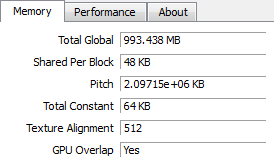
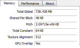
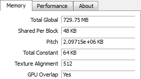
CUDA-Z: CUDA Available Memory. Clockwise, Top-Left: GTS 450, GTX 460 768MB, GTX 550 Ti
At this point NVIDIA tells us it’s a bug and that it should be fixed by the end of the month, however until such a time we’re left with our share of doubts. Although this doesn’t lead to any kind of faulty operation, this is a pretty big bug to slip through NVIDIA’s QA process, which makes it all the more surprising.
In the meantime we did do some testing against the more limited memory capacity of the GTX 550. At this point the results are inconclusive at best. Using NVIDIA’s Bandwidth Test CUDA sample program, which is a simple test to measure memcopy bandwidth of the GPU, we tested the GTS 450, GTX 468 768MB, GTX 460 1GB, and GTX 550 Ti at both stock and normalized (GTX 460) clocks. The results were inconclusive – the test seems to scale with core clocks far more than memory bandwidth – which may be another bug, or an artifact of the program having originally been written pre-Fermi. In any case here is the data, but we have low confidence in it.
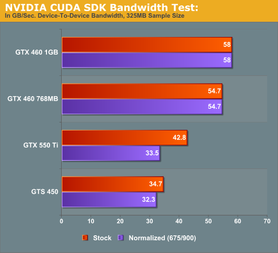
As it stands the test shows almost no gain over the GTS 450 at normalized clocks; this doesn’t make a great deal of sense under any memory interleaving scheme, hence the low confidence. If and when all the bugs that may be causing this are fixed, we’ll definitely be revisiting the issue to try to better pin down how NVIDIA is doing memory interleaving.


79 Comments
View All Comments
HangFire - Tuesday, March 15, 2011 - link
For a while, AT listened and included the 8800GT with most tests. This was a great baseline as most people understood where their card fell in, compared to the 8800GT.AT has since decided (again) that all of us play nothing but the latest Dx11 games in Dx11 mode with all the goodies turned on, and the only folks upgrading already own Dx11 cards anyway.
mapesdhs - Tuesday, March 15, 2011 - link
Very true!
I've been collating performance results to compare older cards to newer
models as and when I can. Google: "Ian PC Benchmarks", it's the first link
that comes back (Blinkenlights site), then select, "PC Benchmarks, Advice
and Information". Note though that Blinkenlights is a mirror, my main site at
sgidepot is always updated first and more often.
I've included lots of 8800GT, 4890 and GTX 460 1GB data so far and I've
just obtained a 9800GT, 3850 AGP (should be a giggle!) and intend to obtain
various other older cards, including a GTX 275/285. I also have an X1950
Pro AGP (don't giggle, I got better results than reviews of the PCIe version).
Platform wise, I'm trying to put together a socket 775 build and also an
AM2/AM3 setup (I've already obtained a Core2Duo 6850 and Q6600
Core2Quad, though no mbd yet). And I'm adding further P55 examples, eg.
I've obtained an i5 670 and will be including an i5 760 aswell. All this done
on a stupid small budget btw (eBay madness), so if anyone has S775 or
AM2 parts they don't want, feel free to contact me. eBay is not exactly
bargain central anymore. :\ If you're after the highest price though, eBay
is best. Or of course free donations are welcome! 8) (I'll cover the postage;
I'm in the UK) I want to create a spread of data that will be genuinely useful
to people.
I don't have Crysis or Metro33 to test with, but I've used a good range of
freely available tests (recommendations welcome; I'm not going to use AVP
though - I had a look, thought it was rather poor). When I have the time I'll
also add real game tests using my own tests, focusing more on older titles
as that's a common issue people have (I'll be testing with Oblivion, the
1st Stalker game, CoD WAW and a few others).
I'm also including pro apps as & when I can since I do have a number of
borrowed Quadro FX cards to test aswell (580, 1500, 1700, 4500, 5500,
5600, etc.) which will all be for sale once the tests are done. So far I've
done some tests on the 1500 and 5500, but until I sort out a proper certified
X58 setup (for SLI) the results won't be fully fleshed out (Dell T7500
barebones on its way, need parts). Interesting to compare gamer & pro cards.
Note that I'm not massively familiar with older gfx cards, so suggestions are
welcome as to what I should include and/or look for. Feel free to email with
ideas (contact page is on my site, just email my Yahoo acccount). Don't post
here though as that'll only clog up the thread.
Lastly, I'm also putting together a standard X58 setup in a little while, but
first I want to sort out the older systems.
Oh, for those commenting about DX11 on older cards, that's absolutely
true, which is why whenever possible I run each test in all three modes,
ie. DX9, DX10 and DX11.
Ian.
PS. If there happens to be anybody in the Edinburgh area who has a card
they'd be willing to lend me so I can add results for it, please let me know.
You can visit and see for yourself. I'm in the Corstorphine/Clermiston area.
medi01 - Tuesday, March 15, 2011 - link
At least this time it doesn't make you color blind, and bar colors make sense (on most charts) unlike in AMD notebook review.Samus - Tuesday, March 15, 2011 - link
...but so does the GTX460. The 550 comes close to the 'stock' 460 when it is radically overclocked, just as the 460 can beat $200+ cards when it is radically overclocked.I appriciate the overclocking 'potential' and coverage, but ever since the eVGA GTX460 FTW review, AT has been dilluting the true nature of these products with overclocked cards carrying heavier weight in the charts than they should.
Your older reviews (<2009) always had a overclock section, omiting the overclocked nature from the rest of the charts. I liked that.
I just don't like seeing overclocked cards reviewed. They are limited runs and YMMV; the eVGA 460 FTW was available for less than a month after you reviewed it, and has since been replaced twice with the Superclocked, and now the Superclocked Extreme Edition, all of which has had varying GPU/BUS/MEM clocks at prices in excess of $80 over the stock cards. That's BS.
mapesdhs - Tuesday, March 15, 2011 - link
Actually the FTW is still easily available, I bought another two last week for a PC I'm
building for a friend.
Ian.
Ryan Smith - Tuesday, March 15, 2011 - link
A lot has changed since 2009. The biggest of which is that NV and AMD have both given manufacturers more freedom in their designs, and simultaneously manufacturers have been looking to further differentiate their products beyond the cooler and price. Factory overclocks are how they're doing it - it allows them to build a card with a higher performance level for little extra cost, increasing their gross margin while filling small holes in the market.Truth be told it creates a bit of a hassle for us as this results in a different card/clock combo every $10, but clearly it's an effective strategy for the manufacturers. At the same time I get why it frustrates you guys, which is why we don't include these cards on our long run charts. But when it comes to reviewing custom cards it's going to be rare to see cards without a factory overclock - most enthusiast cards now have a factory overclock, and what the manufacturers are willing to sample.
On the plus side, as mapesdhs has already noted, manufacturers are getting better about availability. These cards will never have the kind of long term availability that reference clocked cards do (largely due to the fact that it's a single supplier versus many), but many of them are available through the primary market lifetime of the card (which is to say until it's replaced by a newer GPU).
mapesdhs - Tuesday, March 15, 2011 - link
Has to be said though, I didn't expect the FTW to still be that easily available,
but it is.
However, the earlier poster is also correct that there are slightly lower clocked
alternatives from EVGA that cost less, in one case the core/shader clocks are
the same, just a bit slower RAM (the SSC version). Shop around, and note that
sometimes minor differences in prices can be negated by varying shipping costs
between suppliers. I know one company that keeps offering 'special' deals, but
their shipping costs are so high that they're usually more expensive overall than
alternative sources.
I bought the FTWs because that's what my friend wanted, basically a replica
of the system I built for myself.
Ian.
DrPop - Tuesday, March 15, 2011 - link
I love this site and all the reviews are generally very good.However, I am at a loss as to why this and all other GPU reviewers still use aged compute benchmarks such as folding @ home, etc.
Could you PLEASE start running some BOINC tests with QUALITY, optimized, MODERN code for the latest GPUs, so that the world can see the real "number crunching power" each GPU possesses?
Examples of this would be DNETC on BOINC (highly optimized), or Collatz, etc.
I am quite sure you will be surprised at how the computing bar graph will look - it will be very different than the graphs that come out of your current, aged compute code suite.
Thank you!
Ryan Smith - Tuesday, March 15, 2011 - link
It's true Dnetc is highly optimized (and I use it as a torture test because of that) but it's actually kind of a poor benchmark. It's purely compute bound to the point where cache, memory, etc have no impact. For our compute tests we want benchmarks that stress all aspects of the GPU, so that means it not only needs to be compute intensive, but memory intensive, cache sensitive, etc. Otherwise it's just a proxy for GFLOPs and a best case scenario for the VLIW5 architecture.With that said, I am completely open to suggestions. If you know of other programs that offer a decent benchmark and work on AMD and NVIDIA GPUs, I'd like to hear about it. We'll be refreshing the suite in the next couple of months, so now is the time to make suggestions.
HangFire - Tuesday, March 15, 2011 - link
At least the new 550 is marginally faster and lower power idle than the 450. Someone buying-up from one to the other will get a small boost, and even if power demands are slightly higher, the difference is so small that they shouldn't have to buy a new power supply. If they complain they didn't get a big boost, well, buy something with a larger second digit.After all the naming shenanigans Nvidia has played in the past, they should be commended for (at least) getting the name of the card right.
Memory bandwidth is a very important buying comparison for me. I only buy middle end cards with higher than 50GB/s bandwidth, and high end with more than 100GB/s. This is a form of future proofing. I know I can always turn down detail and still get the frame rates (unless it is a very poorly written game). I would settle for 98GB/s. I would not settle for 32GB/s, or some and some.
Oh, yeah, still no comment from AT on intro-time Linux driver support. Why not at least ask, why give Nvidia shelter on this point?