NVIDIA's GeForce GTX 560 Ti: Upsetting The $250 Market
by Ryan Smith on January 25, 2011 9:00 AM ESTThe GF104/GF110 Refresher: Different Architecture & Different Transistors
For all practical purposes GF100 is the Fermi base design, but for sub high-end cards in particular NVIDIA has made a number of changes since we first saw the Fermi architecture a year and a half ago. For those of you reading this article who don’t regularly keep up with the latest NVIDIA hardware releases, we’re going to quickly recap what makes GF114 and GTX 560 Ti different from both the original GF100/GF110 Fermi architecture, and in turn what makes GF114 different from GF104 through NVIDIA’s transistor optimizations. If you’re already familiar with this, please feel free to skip ahead.
With that said, let’s start with architecture. The GF100/GF110 design is ultimately the compute and graphics monster that NVIDIA meant for Fermi to be. It has fantastic graphical performance, but it also extremely solid GPU computing performance in the right scenarios, which is why GF100/GF110 is the backbone of not just NVIDIA’s high-end video cards, but their Tesla line of GPU computing cards.
But Fermi’s compute characteristics only make complete sense at the high-end, as large institutions utilizing GPU computing have no need for weaker GPUs in their servers, and in the meantime home users don’t need features like ECC or full speed FP64 (at least not at this time) so much as they need a more reasonably priced graphics card. As a result only the high-end GF100/GF110 GPUs feature Fermi’s base design, meanwhile GF104 and later use a tweaked design that stripped away some aspects of Fermi’s GPU compute design while leaving much of the graphics hardware intact.
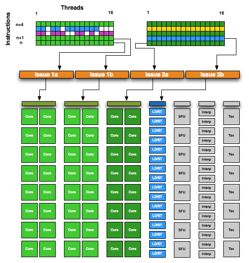
NVIDIA GF104 SM

With GF104 we saw the first GPU released using NVIDIA’s streamlined Fermi architecture that forms the basis of GF104/GF106/GF108/GF114, and we saw a number of firsts from the company. Chief among these was the use of a superscalar architecture, the first time we’ve seen such a design in an NVIDIA part. Superscalar execution allows NVIDIA to take advantage of Instruction Level Parallelism (ILP) – executing the next instruction in a thread when it doesn’t rely on the previous instruction – something they haven’t done previously. It makes this streamlined design notably different from the GF100/GF110 design. And ultimately this design is more efficient than GF100/GF110 on average, while having a wider range of best and worst case scenarios than GF100/GF110, a tradeoff that doesn’t necessarily make sense for GPU computing purposes but does for mainstream graphics.
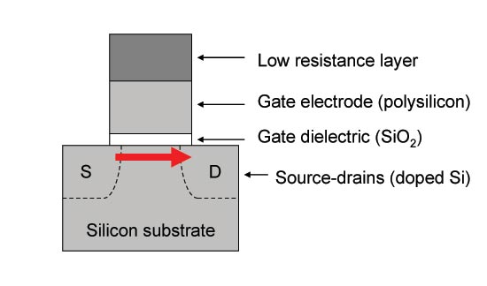
Meanwhile in terms of low-level design, starting with GF110 NVIDIA began revising the low-level design of their GPUs for production purposes. NVIDIA’s choice of transistors with GF10x was suboptimal, and as a result they used leaky transistors in functional units and parts thereof where they didn’t want them, limiting the number of functional units they could utilize and the overall performance they could achieve in the power envelopes they were targeting.
For GF110 NVIDIA focused on better matching the types of transistors they used with what a block needed, allowing them to reduce leakage on parts of the chip that didn’t require such fast & leaky transistors. This meant not only replacing fast leaky transistors with slower, less leaky transistors in parts of the chip that didn’t require such fast transistors, but also introducing a 3rd mid-grade transistor that could bridge the gap between fast/slow transistors. With 3 speed grades of transistors, NVIDIA was able to get away with only using the leakiest transistors where they needed to, and could conserve power elsewhere.

A typical CMOS transitor: Thin gate dielectrics lead to leakage
GF110 wasn’t the only chip to see this kind of optimization however, and the rest of the GF11x line is getting the same treatment. GF114 is in a particularly interesting position since as a smaller GPU, its predecessor GF104 wasn’t as badly affected. Though we can’t speak with respect to enabling additional functional units, at the clockspeeds and voltages NVIDIA was targeting we did not have any issues with the stock voltage. In short while GF100 suffered notably from leakage, GF104 either didn’t suffer from it or did a good job of hiding it. For this reason GF114 doesn’t necessarily stand to gain the same benefit.
As we touched on in our introduction, NVIDIA is putting their gains here in to performance rather than power consumption. The official TDP is going up 10W, while performance is going up anywhere between 10% and 40%. This is the only difference compared to GF104, as GF114 does not contain any architectural changes (GF110’s changes were backported from GF104). Everything we see today will be a result of a better built chip.


87 Comments
View All Comments
martixy - Tuesday, January 25, 2011 - link
Looks quite good.Would get it for the GP compute power just as much as the pixel-pushing power.
I just question the end price in my little corner of the world. :) Most likely it will be double that($249). 250 I can do, 500 - nah... Go figure.
tonyblair - Tuesday, January 25, 2011 - link
Ah, do my eyes decieve me or has good old Anandtech gone back to using bog standard reference GTX460's for Nvidia launches? Haha.mapesdhs - Wednesday, January 26, 2011 - link
Yeah, it's kinda lame, given nobody in their right mind would buy a stock 460
anymore. Many places don't even sell them now, and a highly oc'd 460 is
easily $50 to $60 less than a 560, so a proper comparison would be useful.
Alas, they succumbed to the moaning minnies.
If anyone's interested, I can run the downloadable Stalker COP benchmark
using this review's settings (my own 460 FTW tests have been using 1920x1080,
Extreme detail, SSAO = Default/High, Enhanced Full Dynamic Lighting, so not
directly comparable).
I can't test 2560x1600, but I can test 1680x1050 and 1920x1200, also with
FTW SLI.
Ryan, what full settings did you use for the Stalker test? ie. the SSAO (or
other) mode, etc.?
Ian.
JimmiG - Wednesday, January 26, 2011 - link
I agree.. GTX460 cards are available at speeds up to 850MHz or perhaps even more, a huge difference from the 675MHz that the card supposedly launched at (though even at launch, cards running at anything under 7xx MHz was pretty rare).Parhel - Wednesday, January 26, 2011 - link
Ha! I just bought a stock 460 1GB two weeks ago. Terribly cheap cooler, so the thing only OC's to about 750Mhz before it throttles and I have to reboot. But I only paid $130, so I'm thrilled with the card. I'm on 2560x1600 screen, otherwise the 768MB card would have been the better value.overzealot - Tuesday, January 25, 2011 - link
I remember the Geforce 2 Ti, back in 2001.It wasn't the highest end offering then, either - but it sure was a great cost/performance offer.
It's so bad!
Belard - Thursday, January 27, 2011 - link
The GF2ti was really a die-shrink GF2Pro at 50Mhz faster GPU clock, nothing more. In the real world, it was cheaper than the GF2Pro and was a new CHIP process/series they used for the GF3-TI series. Still, the GF2ti was a pretty good deal in its day at about $125 or so... far cheaper than the $300 GT2-Ultra which just lost its crown to the GF3 series.A little history lesson.
All GF400mx /4000mx series are GF2 technology built on a smaller process, nothing more. Sadily, even now, you can STILL buy NEW GF2mx and GF4000MX cards. The 4000MX is a Frankenstein card. Nvidia took a very slow GF2mx GPU and stuck in DX8...
Check out the stats on Wikipedia - (Basic mid-range cards $200~250)
GF2ti (2001 - 10 years ago) = Fillrate = 00.2 GT/s Bandwidth = 006.4 GB/s DX7
GF4 4200 TI (2002 favorite) = Fillrate = 00.2 GT/s Bandwidth = 008.0 GB/s DX8
GF 6600GT (2004 favorite) = Fillrate = 04.0 GT/s Bandwidth = 014.0 GB/s DX9
GF GTX 260 (2008 favorite) = Fillrate = 41.4 GT/s Bandwidth = 112.0 GB/s DX10
GF GTX 560 (2011 Today) = Fillrate = 52.6 GT/s Bandwidth = 128.2 GB/s DX11
*While the fillrate of GF2 & GF4 are the same, GF2 is a DX7 card, so the GF4 might do the DX7 benchmark at 0.3~.4.
Wow, bandwidth wise, the 560 is 20x faster than the old GF2. Graphic Texture Fillrate is way beyond what those old GF2~4 cards could handle.
Hence, playing Crysis on 560 in 1280x1024 could be around 65fps, on a GF6600, it would be under 10fps with LOW details and maybe 1 frame every 6~10 seconds on the GF2... :)
Lepton87 - Wednesday, January 26, 2011 - link
This card hardly even caught up to my over-a-year-old Radeon 5870. I don't know why this card looks comparatively slow in anandtech's reviews whilst on other tech sites it is about on par with 6950 and thus ever-so-slightly faster then 560Ti.http://www.techpowerup.com/reviews/NVIDIA/GeForce_...
so far I find those charts the most informative when it comes to relative performance between cards. It looks like anandtech's blend of games somewhat favor NV hardware.
SolMiester - Wednesday, January 26, 2011 - link
This is a mid range card that in some benchies surpasses your high previous generation card, at a cheaper price, is quieter and smaller to boot. What more do you want?MeanBruce - Wednesday, January 26, 2011 - link
The Asus 560 looks really amazing, guess it's faster than my brand new Asus 6870 directcu, but that's ok I knew the 560 was coming out, and wanted the Asus 6870 for it's beautiful triple heatpipe and gorgeous backplate heatsink the way it looks thru the window of the Corsair Obsidian 650D. Yup it's not out yet, April but man thru that window with my new Corsair AX850! I'm just buying parts for a window! Oh man the sweetness, that view while I work with Microsoft Word. The 6870 came with dual full sized DisplayPorts fantastic, but the Asus 560 comes with just a mini-HDMI. What is that all about? I didn't even know they came in mini. Maybe AMD will release the 7000 series early this year die shrink and all, 7870 for Christmas ahhh life is good.