NVIDIA's GeForce GTX 560 Ti: Upsetting The $250 Market
by Ryan Smith on January 25, 2011 9:00 AM ESTAs unfathomable as it seems now, at one point in history the product refresh cycle for GPUs was around 6 months. Twice a year NVIDIA and AMD would come out with major refreshes to their product lines, particularly at the high-end where a quick succession of parts brought great performance gains and left us little time to breathe.
Since then things have changed a great deal. GPU complexity has grown by leaps and bounds – although by the time the term “GPU” was even coined GPUs ceased being simple devices, they were still fairly small chips put together at a block level by a relatively small team of engineers. The modern GPU on the other hand is a large, complex entity. Although the development cycle for a GPU is still shorter than the 4+ years for a CPU, GPU complexity has approached the CPU in some ways and exceeded it in others. Meanwhile in terms of die size even midrange GPUs like GF106 (GTS 450) are as big as modern CPUs like Sandy Bridge, never mind high-end GPUs like GF110. As a result the refresh cycle for GPUs has become progressively longer by relying primarily on die shrinks, and in modern times we’re looking at close to a year between refreshes.
The reason I bring this up is because NVIDIA has found itself in an interesting position with the Fermi architecture. We’ve covered the problems NVIDIA had in the past, particularly with the first Fermi – GF100. NVIDIA since corrected GF100’s biggest production flaws in GF110, giving us the Fermi we originally expected nearly half a year earlier. NVIDIA is now in the process of cascading those production improvements down the rest of the Fermi line, churning out the fully-enabled Fermi GPUs that we did not get to see in 2010. Whether it’s intentional or not – and we believe it’s not – NVIDIA has fallen back in to the 6 month cycle.
Late last year we saw GF110, the first of the revised Fermi family. GF110 brought with it GTX 580 and GTX 570, a pair of powerful if expensive video cards that put NVIDIA back where they traditionally lie on the performance/power curve. Now it’s time for GF104 to get the same treatment. Its revised counterpart is the aptly named GF114, and it is the heart of NVIDIA’s newest video card: the GeForce GTX 560 Ti.
| GTX 580 | GTX 570 | GTX 560 Ti | GTX 460 1GB | |
| Stream Processors | 512 | 480 | 384 | 336 |
| Texture Address / Filtering | 64/64 | 60/60 | 64/64 | 56/56 |
| ROPs | 48 | 40 | 32 | 32 |
| Core Clock | 772MHz | 732MHz | 822MHz | 675MHz |
| Shader Clock | 1544MHz | 1464MHz | 1644MHz | 1350MHz |
| Memory Clock | 1002MHz (4008MHz data rate) GDDR5 | 950MHz (3800MHz data rate) GDDR5 | 1002Mhz (4008MHz data rate) GDDR5 | 900Mhz (3.6GHz data rate) GDDR5 |
| Memory Bus Width | 384-bit | 320-bit | 256-bit | 256-bit |
| Frame Buffer | 1.5GB | 1.25GB | 1GB | 1GB |
| FP64 | 1/8 FP32 | 1/8 FP32 | 1/12 FP32 | 1/12 FP32 |
| Transistor Count | 3B | 3B | 1.95B | 1.95B |
| Manufacturing Process | TSMC 40nm | TSMC 40nm | TSMC 40nm | TSMC 40nm |
| Price Point | $499 | $349 | $249 | ~$160 |
GTX 560 Ti, in a nutshell, is a complete video card using the GF104 design; it is to GTX 460 what GTX 580 was to GTX 480. With the GTX 460 we saw NVIDIA disable some functional units and limit the clockspeeds, but for GTX 560 Ti they’re going all out. Every functional unit is enabled, and clockspeeds are much higher, with a core clock of 822MHz being what we believe is much closer to the original design specifications of GF104. Even though GF114 is identical to GF104 in architecture and the number of functional units, as we’re going to see the resulting video cards are quite different – GTX 560 Ti is quite a bit faster than GTX 460 most of the time.
NVIDIA GF114 - Full Implementation, No Disabled Logic
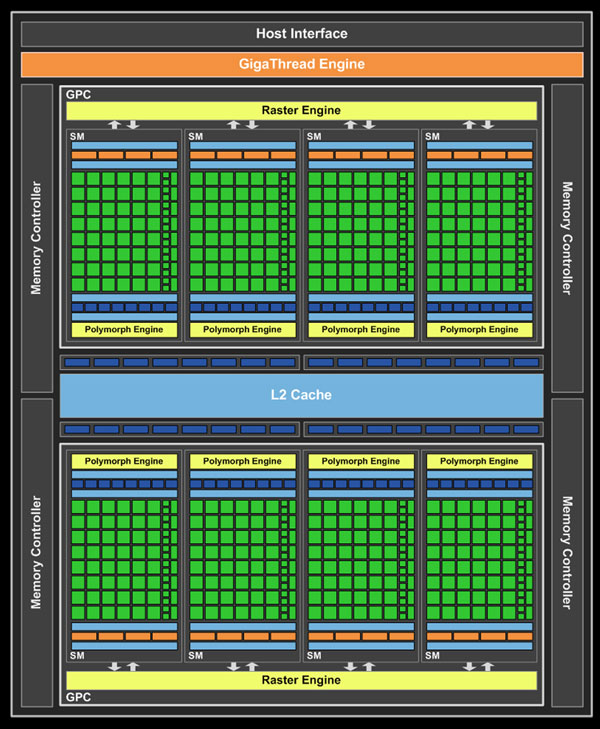
So how is NVIDIA accomplishing this? Much like what GF110 did for GF100, GF114 is doing for GF104. NVIDIA has resorted to tinkering with the Fermi family at a low level to optimize their designs against TSMC’s mature 40nm process, paying much closer attention to the types of transistors used in order to minimize leakage. As a result of the more mature manufacturing process and NVIDIA’s optimizations, they are now able to enable previously disabled functional units and raise clock speeds while keeping these revised GPUs in the same power envelopes as their first-generation predecessors. This is allowing NVIDIA to improve performance and/or power consumption even though these revised chips are virtually identical to their predecessors.
On GF110, we saw NVIDIA choose to take moderate gains in both performance and power consumption. In the case of GF114/GTX 560 however, NVIDIA is choosing to focus on improving performance while leaving power consumption largely unchanged – GTX 460 after all was a well-balanced part in the first place, so why change what already works?
In order to achieve the larger performance jump they’re shooting for, NVIDIA is tackling this from two sides. First of course is the enabling of previously disabled functional units – GTX 460 1GB had all 32 of its ROPs and associated hardware enabled, but only 7 of its 8 SMs enabled, leaving its geometry/shading/texturing power slightly crippled from what the GF104 chip was fully capable of. Like GF110/GTX 580, GF114/GTX 560 Ti will be a fully enabled part: all 384 CUDA Cores, 64 texture units, 8 Polymorph Engines, 32 ROPs, 512KB L2 cache, 4x64bit memory controllers are present, accounted for, and functional. Thus compared to GTX 460 1GB in particular, GTX 560 Ti immediately has more shading, texturing, and geometry performance than its predecessor, with roughly a 14% advantage over a similarly clocked GTX 460 1GB.
The other aspect of improving performance is improving the clockspeed. As you may recall GTX 460 was quite the charming overclocking card, as even without GPU overvolting we could routinely get 20% or more over the stock clock speed of 675MHz; to the point where NVIDIA tried to make an unofficial product out of partner cards with these lofty overclocks. For GTX 560 Ti NVIDIA has rolled these clocks in to the product, with GTX 560 Ti shipping at an 822MHz core clock and 1002MHz (4008MHz data rate) memory clock. This represents a 147Mhz (22%) core clock increase, and a more mild 102MHz (11%) memory clock increase over the GTX 460 1GB. Coupled with the aforementioned 14% increase in SMs, and it’s clear that there’s a quite a potential performance improvement for the GTX 560 even though we’re still technically looking at the same GPU.
As NVIDIA is not looking to significantly move the power envelope on the GTX 560 Ti compared to the GTX 460 1GB, the TDP remains similar. NVIDIA never specifies an idle TDP, but with their transistor level changes it should be lower. Meanwhile load TDP is going up by 10W, from 160W on the GTX 460 1GB to 170W on the GTX 560 Ti. 10W shouldn’t make for a significant difference, but it does drive home the point that NVIDIA is focusing more on performance at the slight expense of power this time around. GF114 is pin compatible with GF104, so partners can drop it in to existing GTX 460 designs, but those designs will need to be able to handle the extra power draw and heat. NVIDIA’s own reference design has been bulked up some, as we’ll see when we dissect the card.
The GTX 560 Ti will be launching at $249, roughly $20 higher than where the GTX 460 1GB started out but still targeted towards the same 1920x1200/1920x1080 resolution user base. Furthermore NVIDIA’s product stack will be shifting in response to the GTX 560 Ti. GTX 460 1GB is officially being moved down to make room for the GTX 560 Ti, and while NVIDIA isn’t providing MSRPs for it, the GTX 460 1GB can be found for as little as $150 after rebates right now – though this is largely a consequence of pricing wars with the AMD 6800 series rather than NVIDIA’s doing. Filling this nearly $100 gap for now will be factory overclocked GTX 460 1GBs. Meanwhile between the GTX 560 and GTX 570 will be a number of factory overclocked GTX 560s launching on day 1 (reusing GTX 460 designs). The GTX 470 is still on the market (and at prices below the GTX 560 for obvious reasons), but it’s not an official part of the stack and we expect supplies to dry up in due time.
NVIDIA’s marketing focus for the GTX 560 is to pair it with Intel’s recently launched Sandy Bridge CPUs, which have inspired a wave of computer upgrades that NVIDIA would like to hitch a ride with. Compared to the GTX 460 the GTX 560 isn’t a major upgrade on its own, and as a result NVIDIA is focusing more towards people upgrading their 8000/9000/GTX200 series equipped computers. Ultimately if you’re upgrading, NVIDIA would love to sell you a $250 GPU alongside a cheaper Core i5 2500K processor.
Meanwhile over at AMD they are shuffling their lineup and launching their own two-front counter-offensive. In terms of pricing and performance the GTX 560 Ti is between the Radeon HD 6950 and Radeon HD 6870, leaving AMD with a hole to fill. AMD has chosen to launch 1 new product – the Radeon HD 6950 1GB – to sit right above the GTX 560 Ti at $259, and in a move similar to how NVIDIA handled the Radeon HD 6800 series launch, push factory overclocked Radeon HD 6870s to go right below the GTX 560 Ti at around $230. The net result is that the price of reference-clocked 6870s has come down nearly $30 from launch, and can now be found for as little as $200. In any case, as there’s a great deal to discuss here, please see our companion article for the full-rundown on AMD’s GTX 560 Ti counter-offensive.
| Early 2011 Video Card MSRPs | ||
| NVIDIA | Price | AMD |
| $500 | ||
| $350 | Radeon HD 6970 | |
| $279-$299 | Radeon HD 6950 2GB | |
|
|
$259 | Radeon HD 6950 1GB |
|
GeForce GTX 560 Ti
|
$249 | |
| $219 | Radeon HD 6870 | |
| $160-170 | Radeon HD 6850 | |


87 Comments
View All Comments
martixy - Tuesday, January 25, 2011 - link
Looks quite good.Would get it for the GP compute power just as much as the pixel-pushing power.
I just question the end price in my little corner of the world. :) Most likely it will be double that($249). 250 I can do, 500 - nah... Go figure.
tonyblair - Tuesday, January 25, 2011 - link
Ah, do my eyes decieve me or has good old Anandtech gone back to using bog standard reference GTX460's for Nvidia launches? Haha.mapesdhs - Wednesday, January 26, 2011 - link
Yeah, it's kinda lame, given nobody in their right mind would buy a stock 460
anymore. Many places don't even sell them now, and a highly oc'd 460 is
easily $50 to $60 less than a 560, so a proper comparison would be useful.
Alas, they succumbed to the moaning minnies.
If anyone's interested, I can run the downloadable Stalker COP benchmark
using this review's settings (my own 460 FTW tests have been using 1920x1080,
Extreme detail, SSAO = Default/High, Enhanced Full Dynamic Lighting, so not
directly comparable).
I can't test 2560x1600, but I can test 1680x1050 and 1920x1200, also with
FTW SLI.
Ryan, what full settings did you use for the Stalker test? ie. the SSAO (or
other) mode, etc.?
Ian.
JimmiG - Wednesday, January 26, 2011 - link
I agree.. GTX460 cards are available at speeds up to 850MHz or perhaps even more, a huge difference from the 675MHz that the card supposedly launched at (though even at launch, cards running at anything under 7xx MHz was pretty rare).Parhel - Wednesday, January 26, 2011 - link
Ha! I just bought a stock 460 1GB two weeks ago. Terribly cheap cooler, so the thing only OC's to about 750Mhz before it throttles and I have to reboot. But I only paid $130, so I'm thrilled with the card. I'm on 2560x1600 screen, otherwise the 768MB card would have been the better value.overzealot - Tuesday, January 25, 2011 - link
I remember the Geforce 2 Ti, back in 2001.It wasn't the highest end offering then, either - but it sure was a great cost/performance offer.
It's so bad!
Belard - Thursday, January 27, 2011 - link
The GF2ti was really a die-shrink GF2Pro at 50Mhz faster GPU clock, nothing more. In the real world, it was cheaper than the GF2Pro and was a new CHIP process/series they used for the GF3-TI series. Still, the GF2ti was a pretty good deal in its day at about $125 or so... far cheaper than the $300 GT2-Ultra which just lost its crown to the GF3 series.A little history lesson.
All GF400mx /4000mx series are GF2 technology built on a smaller process, nothing more. Sadily, even now, you can STILL buy NEW GF2mx and GF4000MX cards. The 4000MX is a Frankenstein card. Nvidia took a very slow GF2mx GPU and stuck in DX8...
Check out the stats on Wikipedia - (Basic mid-range cards $200~250)
GF2ti (2001 - 10 years ago) = Fillrate = 00.2 GT/s Bandwidth = 006.4 GB/s DX7
GF4 4200 TI (2002 favorite) = Fillrate = 00.2 GT/s Bandwidth = 008.0 GB/s DX8
GF 6600GT (2004 favorite) = Fillrate = 04.0 GT/s Bandwidth = 014.0 GB/s DX9
GF GTX 260 (2008 favorite) = Fillrate = 41.4 GT/s Bandwidth = 112.0 GB/s DX10
GF GTX 560 (2011 Today) = Fillrate = 52.6 GT/s Bandwidth = 128.2 GB/s DX11
*While the fillrate of GF2 & GF4 are the same, GF2 is a DX7 card, so the GF4 might do the DX7 benchmark at 0.3~.4.
Wow, bandwidth wise, the 560 is 20x faster than the old GF2. Graphic Texture Fillrate is way beyond what those old GF2~4 cards could handle.
Hence, playing Crysis on 560 in 1280x1024 could be around 65fps, on a GF6600, it would be under 10fps with LOW details and maybe 1 frame every 6~10 seconds on the GF2... :)
Lepton87 - Wednesday, January 26, 2011 - link
This card hardly even caught up to my over-a-year-old Radeon 5870. I don't know why this card looks comparatively slow in anandtech's reviews whilst on other tech sites it is about on par with 6950 and thus ever-so-slightly faster then 560Ti.http://www.techpowerup.com/reviews/NVIDIA/GeForce_...
so far I find those charts the most informative when it comes to relative performance between cards. It looks like anandtech's blend of games somewhat favor NV hardware.
SolMiester - Wednesday, January 26, 2011 - link
This is a mid range card that in some benchies surpasses your high previous generation card, at a cheaper price, is quieter and smaller to boot. What more do you want?MeanBruce - Wednesday, January 26, 2011 - link
The Asus 560 looks really amazing, guess it's faster than my brand new Asus 6870 directcu, but that's ok I knew the 560 was coming out, and wanted the Asus 6870 for it's beautiful triple heatpipe and gorgeous backplate heatsink the way it looks thru the window of the Corsair Obsidian 650D. Yup it's not out yet, April but man thru that window with my new Corsair AX850! I'm just buying parts for a window! Oh man the sweetness, that view while I work with Microsoft Word. The 6870 came with dual full sized DisplayPorts fantastic, but the Asus 560 comes with just a mini-HDMI. What is that all about? I didn't even know they came in mini. Maybe AMD will release the 7000 series early this year die shrink and all, 7870 for Christmas ahhh life is good.