NVIDIA's GeForce GTX 560 Ti: Upsetting The $250 Market
by Ryan Smith on January 25, 2011 9:00 AM ESTThe GF104/GF110 Refresher: Different Architecture & Different Transistors
For all practical purposes GF100 is the Fermi base design, but for sub high-end cards in particular NVIDIA has made a number of changes since we first saw the Fermi architecture a year and a half ago. For those of you reading this article who don’t regularly keep up with the latest NVIDIA hardware releases, we’re going to quickly recap what makes GF114 and GTX 560 Ti different from both the original GF100/GF110 Fermi architecture, and in turn what makes GF114 different from GF104 through NVIDIA’s transistor optimizations. If you’re already familiar with this, please feel free to skip ahead.
With that said, let’s start with architecture. The GF100/GF110 design is ultimately the compute and graphics monster that NVIDIA meant for Fermi to be. It has fantastic graphical performance, but it also extremely solid GPU computing performance in the right scenarios, which is why GF100/GF110 is the backbone of not just NVIDIA’s high-end video cards, but their Tesla line of GPU computing cards.
But Fermi’s compute characteristics only make complete sense at the high-end, as large institutions utilizing GPU computing have no need for weaker GPUs in their servers, and in the meantime home users don’t need features like ECC or full speed FP64 (at least not at this time) so much as they need a more reasonably priced graphics card. As a result only the high-end GF100/GF110 GPUs feature Fermi’s base design, meanwhile GF104 and later use a tweaked design that stripped away some aspects of Fermi’s GPU compute design while leaving much of the graphics hardware intact.
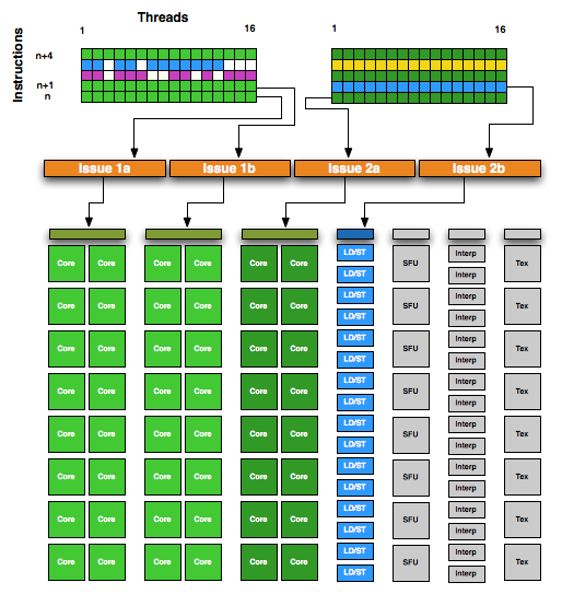
NVIDIA GF104 SM
With GF104 we saw the first GPU released using NVIDIA’s streamlined Fermi architecture that forms the basis of GF104/GF106/GF108/GF114, and we saw a number of firsts from the company. Chief among these was the use of a superscalar architecture, the first time we’ve seen such a design in an NVIDIA part. Superscalar execution allows NVIDIA to take advantage of Instruction Level Parallelism (ILP) – executing the next instruction in a thread when it doesn’t rely on the previous instruction – something they haven’t done previously. It makes this streamlined design notably different from the GF100/GF110 design. And ultimately this design is more efficient than GF100/GF110 on average, while having a wider range of best and worst case scenarios than GF100/GF110, a tradeoff that doesn’t necessarily make sense for GPU computing purposes but does for mainstream graphics.
Meanwhile in terms of low-level design, starting with GF110 NVIDIA began revising the low-level design of their GPUs for production purposes. NVIDIA’s choice of transistors with GF10x was suboptimal, and as a result they used leaky transistors in functional units and parts thereof where they didn’t want them, limiting the number of functional units they could utilize and the overall performance they could achieve in the power envelopes they were targeting.
For GF110 NVIDIA focused on better matching the types of transistors they used with what a block needed, allowing them to reduce leakage on parts of the chip that didn’t require such fast & leaky transistors. This meant not only replacing fast leaky transistors with slower, less leaky transistors in parts of the chip that didn’t require such fast transistors, but also introducing a 3rd mid-grade transistor that could bridge the gap between fast/slow transistors. With 3 speed grades of transistors, NVIDIA was able to get away with only using the leakiest transistors where they needed to, and could conserve power elsewhere.
![]()
A typical CMOS transitor: Thin gate dielectrics lead to leakage
GF110 wasn’t the only chip to see this kind of optimization however, and the rest of the GF11x line is getting the same treatment. GF114 is in a particularly interesting position since as a smaller GPU, its predecessor GF104 wasn’t as badly affected. Though we can’t speak with respect to enabling additional functional units, at the clockspeeds and voltages NVIDIA was targeting we did not have any issues with the stock voltage. In short while GF100 suffered notably from leakage, GF104 either didn’t suffer from it or did a good job of hiding it. For this reason GF114 doesn’t necessarily stand to gain the same benefit.
As we touched on in our introduction, NVIDIA is putting their gains here in to performance rather than power consumption. The official TDP is going up 10W, while performance is going up anywhere between 10% and 40%. This is the only difference compared to GF104, as GF114 does not contain any architectural changes (GF110’s changes were backported from GF104). Everything we see today will be a result of a better built chip.


87 Comments
View All Comments
Nimiz99 - Tuesday, January 25, 2011 - link
One of my buddies has a C2D 8500 system OC'd to 3.5 i think. He got himself a 5870 (overclocked) to game. The problem we ran into was that the C2D is too slow to handle games like Civ5 that heavily rely on the CPU to keep up (you can still play the game, but it's literally wasting the 5870 with noticeable lag from the chip). Basically, he is upgrading now to a sandy bridge. I'd wager some of the older i7's or maybe even a Thuban (OC'd to 3.8 with a good HT overclock) could manage, but why bother when a new architecture is out form Intel (or AMD later in the year).So enjoy your new build ;),
Nimiz
Beenthere - Tuesday, January 25, 2011 - link
Over the last couple years Nvidia has really struggled and they may be on the ropes at this point. They have created a lot of their own problems with their arrogance so we'll see how it all plays out.kilkennycat - Tuesday, January 25, 2011 - link
eVGA GTX560 Ti "Superclocked" Core: 900MHz, Shader 1800MHZ; Memory 4212MHz $279.99~ 10% factory-overclock for $20 extra, together with a lifetime warranty (if you register within 30 days) ain't too shabby....
Belard - Tuesday, January 25, 2011 - link
Sure, the name shouldn't be a big deal... but each year or worse, Nvidia comes up with a new marketing product name that is meaningless and confusing.Here is the full product name:
GeForce GTX 560 Ti But in reality, the only part that is needed or makes ANY sense is:
GeForce 560
GTX / GT / GTs are worthless. Unless there were GTX 560, GTS 560 and GT 560. Much like the older 8800 series.
TI is only added to this idiotic mess. Might as well Ultra, Pro or MX.... so perhaps Nvidia will come out with the "GT 520 mx"?
The product itself is solid, why turn it into something stupid with your marketing department?
AMD does it right (mostly), the "Radeaon 6870" that's it. DUH.
omelet - Tuesday, January 25, 2011 - link
Yeah. Not that it really matters. And while this might be what you meant by "mostly" note that AMD's naming was pretty retarded this generation with the 68xx having lower performance than 58xx.But I don't see why they readopted the Ti moniker.
Sufo - Wednesday, January 26, 2011 - link
no, that's only a result of the 5xxx series being stupidly named. Using 5970 for a dual chip part was the error. Use an x2 suffix or smthng. AMD is back on track with the 6xxx naming convention... well, until we see what they do with the 6 series dual chip card.Belard - Thursday, January 27, 2011 - link
The model numbers of:x600, x800, etc have been consistent since the 3000 series.
x800 is top
x700 is high-end mid range ($200 sub)
x600 is mid-range ($150 sub)
x400~500 low-end ($50~60)
x200~300 Desktop or HTPC cards.
AMD said they changed because they didn't want to confuse people with the 5750/5770 cards with the 6000 series. Which is completely stupid... so instead they confuse everyone with all th cards.
If the 6800s were called 6700s - they would have been easily faster than any of the 5700s and at least somewhat equal to the 5800s (sometimes slower, others faster). Instead, we have "6850" that is slower than the 5850.
The prices are a bit high still, yet far cheaper than the 5800 series, in which a 5850 was $300+ or $400 for the 5870. But by all means, I'd rather spend $220 on a 6870 than $370 on todays 5870s.
Anyways, I'm still using a 4670 in my main computer. When I do my next upgrade, I'll spend about $200 at the most and want at least 6870 level of performance, which is still about 4x faster than what I have now. Noise & heat are very high on my list, my 4670 was $15 extra for the better noise & heat cooling system. Perhaps in 6 months, the AMD 7000 or GeForce 700 series will be out.
marraco - Tuesday, January 25, 2011 - link
Is the first time I see a radiator geometrically aligned to the direction of air velocity thrown by the fan.Obviously it increases the efficiency of the fan, increasing the flow of air thrown across the radiator, and reducing noise.
It’s an obvious enhancement in air cooling, that I don’t understand why CPU coolers don’t use.
strikeback03 - Tuesday, January 25, 2011 - link
I wouldn't be surprised if in some cases the increase in fin surface area (from having a bunch of straight fins packed more closely together) produces better cooling than having a cleaner airpath.MeanBruce - Wednesday, January 26, 2011 - link
You should check out the four Asus Direct CU II three slot radiators that came out today on the GTX 580, 570, and the HD 6970 and 6950, each using two 100mm fans, five heatpipes and three slots of pure metal, they claim you can easily fit two of them on ATX for SLI and CB?