NVIDIA's GeForce GTX 560 Ti: Upsetting The $250 Market
by Ryan Smith on January 25, 2011 9:00 AM ESTThe GF104/GF110 Refresher: Different Architecture & Different Transistors
For all practical purposes GF100 is the Fermi base design, but for sub high-end cards in particular NVIDIA has made a number of changes since we first saw the Fermi architecture a year and a half ago. For those of you reading this article who don’t regularly keep up with the latest NVIDIA hardware releases, we’re going to quickly recap what makes GF114 and GTX 560 Ti different from both the original GF100/GF110 Fermi architecture, and in turn what makes GF114 different from GF104 through NVIDIA’s transistor optimizations. If you’re already familiar with this, please feel free to skip ahead.
With that said, let’s start with architecture. The GF100/GF110 design is ultimately the compute and graphics monster that NVIDIA meant for Fermi to be. It has fantastic graphical performance, but it also extremely solid GPU computing performance in the right scenarios, which is why GF100/GF110 is the backbone of not just NVIDIA’s high-end video cards, but their Tesla line of GPU computing cards.
But Fermi’s compute characteristics only make complete sense at the high-end, as large institutions utilizing GPU computing have no need for weaker GPUs in their servers, and in the meantime home users don’t need features like ECC or full speed FP64 (at least not at this time) so much as they need a more reasonably priced graphics card. As a result only the high-end GF100/GF110 GPUs feature Fermi’s base design, meanwhile GF104 and later use a tweaked design that stripped away some aspects of Fermi’s GPU compute design while leaving much of the graphics hardware intact.
NVIDIA GF104 SM
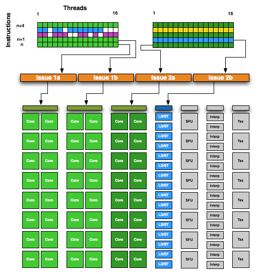
With GF104 we saw the first GPU released using NVIDIA’s streamlined Fermi architecture that forms the basis of GF104/GF106/GF108/GF114, and we saw a number of firsts from the company. Chief among these was the use of a superscalar architecture, the first time we’ve seen such a design in an NVIDIA part. Superscalar execution allows NVIDIA to take advantage of Instruction Level Parallelism (ILP) – executing the next instruction in a thread when it doesn’t rely on the previous instruction – something they haven’t done previously. It makes this streamlined design notably different from the GF100/GF110 design. And ultimately this design is more efficient than GF100/GF110 on average, while having a wider range of best and worst case scenarios than GF100/GF110, a tradeoff that doesn’t necessarily make sense for GPU computing purposes but does for mainstream graphics.
Meanwhile in terms of low-level design, starting with GF110 NVIDIA began revising the low-level design of their GPUs for production purposes. NVIDIA’s choice of transistors with GF10x was suboptimal, and as a result they used leaky transistors in functional units and parts thereof where they didn’t want them, limiting the number of functional units they could utilize and the overall performance they could achieve in the power envelopes they were targeting.
For GF110 NVIDIA focused on better matching the types of transistors they used with what a block needed, allowing them to reduce leakage on parts of the chip that didn’t require such fast & leaky transistors. This meant not only replacing fast leaky transistors with slower, less leaky transistors in parts of the chip that didn’t require such fast transistors, but also introducing a 3rd mid-grade transistor that could bridge the gap between fast/slow transistors. With 3 speed grades of transistors, NVIDIA was able to get away with only using the leakiest transistors where they needed to, and could conserve power elsewhere.
![]()
A typical CMOS transitor: Thin gate dielectrics lead to leakage
GF110 wasn’t the only chip to see this kind of optimization however, and the rest of the GF11x line is getting the same treatment. GF114 is in a particularly interesting position since as a smaller GPU, its predecessor GF104 wasn’t as badly affected. Though we can’t speak with respect to enabling additional functional units, at the clockspeeds and voltages NVIDIA was targeting we did not have any issues with the stock voltage. In short while GF100 suffered notably from leakage, GF104 either didn’t suffer from it or did a good job of hiding it. For this reason GF114 doesn’t necessarily stand to gain the same benefit.
As we touched on in our introduction, NVIDIA is putting their gains here in to performance rather than power consumption. The official TDP is going up 10W, while performance is going up anywhere between 10% and 40%. This is the only difference compared to GF104, as GF114 does not contain any architectural changes (GF110’s changes were backported from GF104). Everything we see today will be a result of a better built chip.


87 Comments
View All Comments
ggathagan - Tuesday, January 25, 2011 - link
I believe you mean "Apparently Anandtech's efforts to find good writers were in vain."phoible4 - Tuesday, January 25, 2011 - link
The GTX560 looks interesting. However, prices for 768MB 460s are hitting rock bottom. I just paid $90 for one from TigerDirect (after rebates), and it looks like there are a few under $130 on Newegg. It seems like it would cost about the same to run SLI 460s and 1 560 (assuming your case can handle it), and I can guess that the SLI config would be faster in most games.I actually kind of expected NVidia to release a dual-chip 460 as their next-gen 580, and take a page out of AMD's playbook (wonder how hot/loud that would be).
Belard - Thursday, January 27, 2011 - link
The GF 460-768mb are slow compared to their 1Gb versions. They run out of memory way too quick. But for $90... that would be a great deal that is worthwhile. Newegg is showing $150 on avg for the 768mb 460s. Which is about $25 less than a newer 6850 card which is easily faster. Its even faster than the 1GB 460 and cost less.mosox - Tuesday, January 25, 2011 - link
[quoteAMD’s scramble to launch the Radeon HD 6950 1GB has produced a card with similar levels of performance and pricing as the GTX 560 Ti, making it impossible to just blindly recommend the GTX 560 Ti.[/quote]What? The 6950 2GB is faster than the 560 and the The 6950 2GB is FASTER than the 6950 2GB at every resolution except the highest ones like 2560x1600.
This is from Tom's:
mosox - Tuesday, January 25, 2011 - link
Read that as The 6950 1GB is FASTER than the 6950 2GB, sorry.Visual - Wednesday, January 26, 2011 - link
you read that right - "tighter memory timings"ritalinkid18 - Tuesday, January 25, 2011 - link
I would just like to say, very nice article... well written and informative. I've been a fan of anandtech for many years and the GPU articles never disappoint.Is it just me or does anyone else find reading about Nvidia's architecture a lot more interesting?
Also, I really hate that the comments are filled with people that say you are bias towards NVIDIA. To all those people, PLEASE go read the some other reviews. A majority of them praise the 560. This article is more critical of the 560 value than most.
jonks - Tuesday, January 25, 2011 - link
"The GTX 560 is always faster than the GTX 470, but never immensely so; and at higher resolutions the GTX 470 still has an advantage."So the 560 is always faster than the 470 except when it's not. :)
poohbear - Tuesday, January 25, 2011 - link
wow the gpu market is definitely intense! nvidia and AMD are neck & neck now, very nice time to buy a vid card!7Enigma - Tuesday, January 25, 2011 - link
Thanks again Ryan and Anandtech for keeping the 4870 in your charts for 1920X1200 res. I've always read the new gpu reviews and been saddened that although the new cards are fast they were still not approaching 2X the performance of my 4870. With the constant name change with the same parts, or slightly faster parts, it's taken until just about now to have a card worth the upgrade.Now my question is will I see the performance improvement in GAMES using my C2D 8500 (OC'd to 3.8GHz), or do I need to rebuild the system with Sandy Bridge to actually see the 2X GPU performance?