NVIDIA's Tegra 2 Take Two: More Architectural Details and Design Wins
by Anand Lal Shimpi on January 5, 2011 2:51 PM EST- Posted in
- Smartphones
- Motorola Droid
- Tegra 2
- LG
- Optimus 2X
- ATRIX 4G
- Mobile
- NVIDIA
The GeForce ULV GPU
Tegra 2 integrates the GeForce ULV, an NVIDIA designed OpenGL ES 2.0 GPU.
At a high level NVIDIA is calling the GeForce ULV an 8-core GPU, however its not a unified shader GPU. Each core is an ALU but half of them are used for vertex shaders and the other half are for pixel shaders. You can expect the GeForce ULV line to take a similar evolutionary path to desktop GeForce in the future.
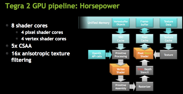
The four vertex shader cores/ALUs can do a total of 4 MADDs per clock, the same is true for the four pixel shader ALUs (4 MADDs per clock).
For those of you who follow NVIDIA’s desktop architecture: at the front end the machine works on a 4-thread warp, where each thread is a single pixel.
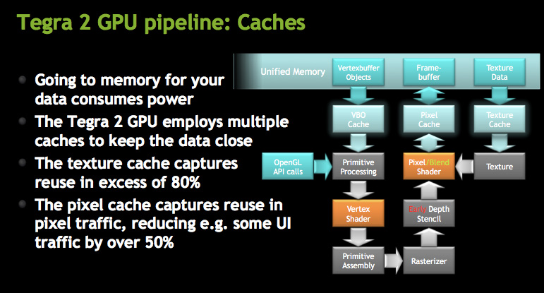
Architecturally, the GeForce ULV borrows several technologies that only recently debuted on desktop GPUs. GeForce ULV has a pixel cache, a feature that wasn’t introduced in GeForce on the desktop until Fermi. This is purely an efficiency play as saving any trips to main memory reduces power consumption considerably (firing up external interfaces always burns watts quicker than having data on die).
NVIDIA also moved the register files closer to the math units, again in the pursuit of low power consumption. GeForce ULV is also extremely clock gated although it’s not something we’re able to quantify.
NVIDIA did reduce the number of pipeline stages compared to its desktop GPUs by a factor of 2.5 to keep power consumption down.
The GeForce ULV supports Early Z culling, a feature first introduced on the desktop with G80. While G80 could throw away around 64 pixels per clock, early Z on GeForce ULV can throw away 4 pixels per clock.
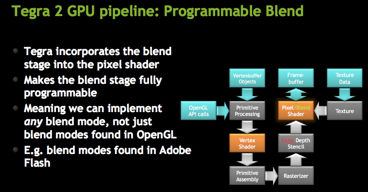
The ROPs are integrated into the pixel shader, making what NVIDIA calls a programmable blend unit. GeForce ULV uses the same ALUs for ROPs as it does for pixel shaders. This hardware reuse saves die size although it adds control complexity to the design. The hardware can perform one texture fetch and one ROP operation per clock.
While GeForce ULV supports texture compression, it doesn’t support frame buffer compression.
Both AA and AF are supported by GeForce ULV. NVIDIA supports 5X coverage sample AA (same CSAA as we have on the desktop) and up to 16X anisotropic filtering.

We’ve done a little bit of performance testing of Tegra 2’s GPU vs. the PowerVR SGX 530/540 and Qualcomm’s Adreno 200/205. It’s too soon for us to publish Tegra 2 smartphone performance numbers, but the numbers NVIDIA is sharing with us show a huge advantage over competitive GPUs. In our own experience we’ve found that Tegra 2’s GPU is a bit faster than the PowerVR SGX 540, but nothing lines up with the numbers NVIDIA has shown us thus far. We’re still a couple of months away from final software and driver builds so it’s possible that things will change.


21 Comments
View All Comments
nahidalam - Wednesday, June 29, 2011 - link
Anand/Brian,Any details on the security engine tegra2 is using?