AMD's Radeon HD 6970 & Radeon HD 6950: Paving The Future For AMD
by Ryan Smith on December 15, 2010 12:01 AM ESTAdvancing Primitives: Dual Graphics Engines & New ROPs
AMD has clearly taken NVIDIA’s comments on geometry performance to heart. Along with issuing their manifesto with the 6800 series, they’ve also been working on their own improvements for their geometry performance. As a result AMD’s fixed function Graphics Engine block is seeing some major improvements for Cayman.
Prior to Cypress, AMD had 1 graphics engine, which contained 1 each of the fundamental blocks: the rasterizers/hierarchical-Z units, the geometry/vertex assemblers, and the tessellator. With Cypress AMD added a 2nd rasterizer and 2nd hierarchical-Z unit, allowing them to set up 32 pixels per clock as opposed to 16 pixels per clock. However while AMD doubled part of the graphics engine, they did not double the entirety of it, meaning their primitive throughput rate was still 1 primitive/clock, a typical throughput rate even at the time.
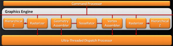
Cypress's Graphics Engine
In 2010 with the launch of Fermi, NVIDIA raised the bar on primitive performance, with rasterization moved to NVIDIA’s GPCs, NVIDIA could theoretically push out as many primitives/clock as they had GPCs, in the case of GF100/GF110 pushing this to 4 primitives/clock, a simply massive improvement in geometry performance for a single generation.
With Cayman AMD is catching up with NVIDIA by increasing their own primitive throughput rate, though not by as much as NVIDIA did with Fermi. For Cayman the rest of the graphics engine is being fully duplicated – Cayman will have 2 separate graphics engines, each containing one fundamental block, and each capable of pushing out 1 primitive/clock. Between the two of them AMD’s maximum primitive throughput rate will now be 2 primitives/clock; half as much as NVIDIA but twice that of Cypress.
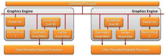
Cayman's Dual Graphics Engines
As was the case for NVIDIA, splitting up rasterization and tessellation is not a straightforward and easy task. For AMD this meant teaching the graphics engine how to do tile-based load balancing so that the workload being spread among the graphics engines is being kept as balanced as possible. Furthermore AMD believes they have an edge on NVIDIA when it comes to design - AMD can scale the number of eraphics engines at will, whereas NVIDIA has to work within the logical confines of their GPC/SM/SP ratios. This tidbit would seem to be particularly important for future products, when AMD looks to scale beyond 2 graphics engines.
At the end of the day all of this tinking with the graphics engines is necessary in order for AMD to further improve their tessellation performance. AMD’s 7th generation tessellator improved their performance at lower tessellation factors where the tessellator was the bottleneck, but at higher tessellation factors the graphics engine itself is the bottleneck as the graphics engine gets swamped with more incoming primitives than it can set up in a single clock. By having two graphics engines and a 2-primitive/clock rasterization rate, AMD is shifting the burden back away from the graphics engine.
Just having two 7th generation-like tessellators goes a long way towards improving AMD’s tessellation performance. However all of that geometry can still lead to a bottleneck at times, which means it needs to be stored somewhere until it can be processed. As AMD has not changed any cache sizes for Cayman, there’s the same amount of cache for potentially thrice as much geometry, so in order to keep things flowing that geometry has to go somewhere. That somewhere is the GPU’s RAM, or as AMD likes to put it, their “off-chip buffer.” Compared to cache access RAM is slow and hence this isn’t necessarily a desirable action, but it’s much, much better than stalling the pipeline entirely while the rasterizers clear out the backlog.
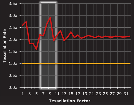
Red = 6970. Yellow = 5870
Overall, clock for clock tessellation performance is anywhere between 1.5x and 3x that of Cypress. In situations where AMD’s already improved tessellation performance at lower tessellation factors plays a part, AMD approaches 3x performance; while at around a factor of 5 the performance drops to near 1.5x. Elsewhere performance is around 2x that of Cypress, representing the doubling of graphics engines.
Tessellation also plays a factor in AMD’s other major gaming-related improvement: ROP performance. As tessellation produces many mini triangles, these triangles begin to choke the ROPs when performing MSAA. Although tessellation isn’t the only reason, it certainly plays a factor in AMD’s reasoning for improving their ROPs to improve MSAA performance.
The 32 ROPs (the same as Cypress) have been tweaked to speed up processing of certain types of values. In the case of both signed and unsigned normalized INT16s, these operations are now 2x faster. Meanwhile FP32 operations are now 2x to 4x faster depending on the scenario. Finally, similar to shader read ops for compute purposes, ROP write ops for graphics purposes can be coalesced, improving performance by requiring fewer operations.


168 Comments
View All Comments
B3an - Thursday, December 16, 2010 - link
Very stupid uninformed and narrow-minded comment. People like you never look to the future which anyone should do when buying a graphics card, and you completely lack any imagination. Theres already tons of uses for GPU computing, many of which the average computer user can make use of, even if it's simply encoding a video faster. And it will be use a LOT more in the future.Most people, especially ones that game, dont even have 17" monitors these days. The average size monitor for any new computer is at least 21" with 1680 res these days. Your whole comment is as if everyone has the exact same needs as YOU. You might be happy with your ridiculously small monitor, and playing games at low res on lower settings, and it might get the job done, but lots of people dont want this, they have standards and large monitors and needs to make use of these new GPU's. I cant exactly see many people buying these cards with a 17" monitor!
CeepieGeepie - Thursday, December 16, 2010 - link
Hi Ryan,First, thanks for the review. I really appreciate the detail and depth on the architecture and compute capabilities.
I wondered if you had considered using some of the GPU benchmarking suites from the academic community to give even more depth for compute capability comparisons. Both SHOC (http://ft.ornl.gov/doku/shoc/start) and Rodinia (https://www.cs.virginia.edu/~skadron/wiki/rodinia/... look like they might provide a very interesting set of benchmarks.
Ryan Smith - Thursday, December 16, 2010 - link
Hi Ceepie;I've looked in to SHOC before. Unfortunately it's *nix-only, which means we can't integrate it in to our Windows-based testing environment. NVIDIA and AMD both work first and foremost on Windows drivers for their gaming card launches, so we rarely (if ever) have Linux drivers available for the launch.
As for Rodinia, this is the first time I've seen it. But it looks like their OpenCL codepath isn't done, which means it isn't suitable for cross-vendor comparisons right now.
IdBuRnS - Thursday, December 16, 2010 - link
"So with that in mind a $370 launch price is neither aggressive nor overpriced. Launching at $20 over the GTX 570 isn’t going to start a price war, but it’s also not so expensive to rule the card out. "At NewEgg right now:
Cheapest GTX 570 - $509
Cheapest 6970 - $369
$30 difference? What are you smoking? Try $140 difference.
IdBuRnS - Thursday, December 16, 2010 - link
Oops, $20 difference. Even worse.IdBuRnS - Thursday, December 16, 2010 - link
570...not 580.../hangsheadinshame
epyon96 - Thursday, December 16, 2010 - link
This was a very interesting discussion to me in the article.I'm curious if Anandtech might expand on this further in a future dedicated article comparing what NVIDIA is using to AMD.
Are they also more similar to VLIW4 or VLIW5?
Can someone else shed some light on it?
Ryan Smith - Thursday, December 16, 2010 - link
We wrote something almost exactly like you're asking for for our Radeon HD 4870 review.http://www.anandtech.com/show/2556
AMD and NVIDIA's compute architectures are still fundamentally the same, so just about everything in that article still holds true. The biggest break is VLIW4 for the 6900 series, which we covered in our article this week.
But to quickly answer your question, GF100/GF110 do not immediately compare to VLIW4 or VLIW5. NVIDIA is using a pure scalar architecture, which has a number of fundamental differences from any VLIW architecture.
dustcrusher - Thursday, December 16, 2010 - link
The cheap insults are nothing but a detriment to what is otherwise an interesting argument, even if I don't agree with you.As far as the intellect of Anandtech readers goes, this is one of the few sites where almost all of the comments are worth reading; most sites are the opposite- one or two tiny bits of gold in a big pan of mud.
I'm not going to "vastly overestimate" OR underestimate your intellect though- instead I'm going to assume that you got caught up in the moment. This isn't Tom's or Dailytech, a little snark is plenty.
Arnulf - Thursday, December 16, 2010 - link
When you launch an application (say a game), it is likely to be the only active thread running on the system, or perhaps one of very few active threads. CPU with Turbo function will clock up as high as possible to run this main thread. When further threads are launched by the application, CPU will inevitably increase its power consumption and consequently clock down.While CPU manufacturers don't advertise this functionality in this manner, it is really no different from PowerTune.
Would PowerTune technology make you feel any better if it was marketed the other way around, the way CPUs are ? (mentioning lowest frequencies and clock boost provided that thermal cap isn't met yet)