VIA's Dual Core Nano & VN1000 Chipset Previewed
by Anand Lal Shimpi on November 15, 2010 12:26 PM ESTI haven’t had an official product briefing with VIA in years. The last time I met with a representative from the company was two years ago outside of IDF in San Francisco. Before then, it was probably around 4 years.
VIA was the first casualty of integration in the PC space. Today we’re all talking about moving graphics onto the processor die, but a few years ago we were having similar discussions about moving the memory controller and north bridge on die. As a manufacturer of chipsets (north and south bridges) for CPUs, VIA lost relevance in the x86 CPU market as the need for a third party chipset maker faded.
VIA’s recent visit to me in Raleigh, NC had two purposes according to the company. One, to remind me that VIA was still around and to give me some face to face time with a VIA representative (appreciated). And two, to showcase VIA’s dual-core Nano platform and brand new integrated graphics chipset (intriguing).
For those of you who don’t know, Nano is VIA’s answer to Atom, except it came along long before Atom did. Just like Atom, Nano was designed in Texas but by VIA’s Centaur team - a microprocessor company it acquired several years back. Centaur’s speciality was low power microarchitectures, and Nano is exactly that.
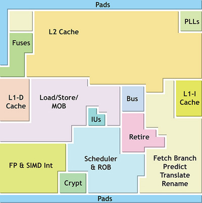
Compared to Atom, Nano is a bit of a beast. Both Atom and AMD’s Bobat core can fetch and issue up to two instructions. Nano can do three. Like AMD’s Bobcat, Nano has a full out of order execution engine. Atom, for the time being, is in-order.
The execution engine is well matched to the front end. Nano features seven dispatch ports and can retire up to three instructions per clock. In this sense, Nano is more like AMD’s Bobcat than Intel’s Atom. In fact, those two should be better matched than Atom vs. Nano.
VIA's Nano
Nano has other advantages over Atom. It features a hardware encryption engine. Something VIA introduced long before Intel’s AES-NI in Westmere. All of these features come at the expense of power consumption. Nano should be faster, but it draws more power than Atom.
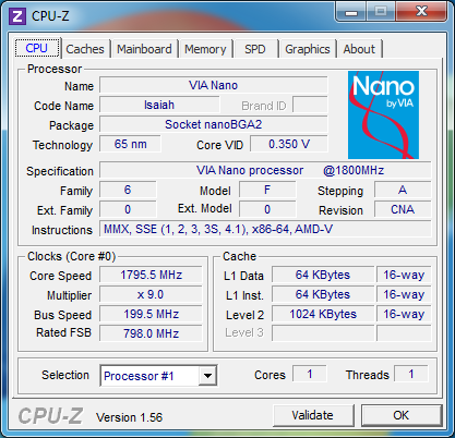
VIA is a fabless semiconductor manufacturer, its Nano processor and associated chipset are both fabbed at TSMC in Taiwan. Nano is currently a 65nm design although VIA plans to take it to 40nm in 2011.
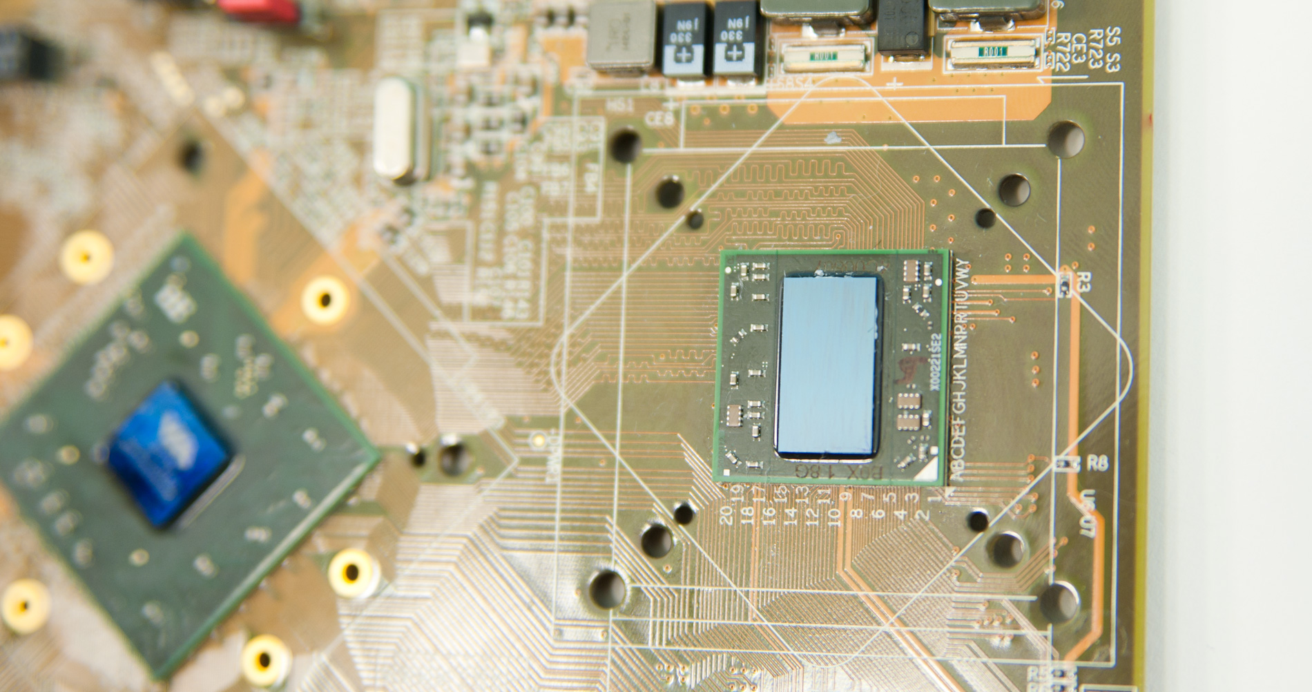
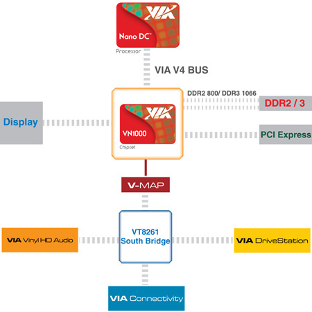
The dual-core Nano that VIA dropped off is architecturally identical to the existing Nano. Similar to the dual-core CPUs, DC Nano is literally two Nano die placed alongside one another. The L2 caches are private and all core-to-core communication happens externally via the Nano’s latest chipset: VIA’s VN1000. The dual-core die measures 8.5 mm x 16 mm (136mm^2 total area) on a 21 mm x 21 mm BGA package.
Ironically enough, VIA hasn’t integrated a memory controller into its own CPU design. Although to VIA’s credit, the CPU’s performance is competitive without it. I suspect VIA will deliver a more integrated version of Nano within the next 12 - 18 months.
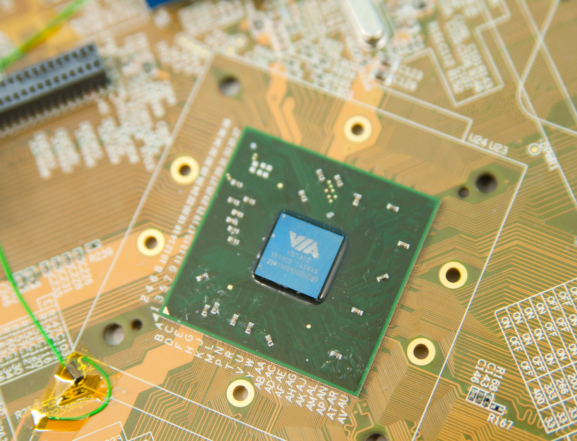
While the dual core Nano improves competitiveness with Intel’s Atom, it’s the VN1000 that’s a huge step forward. These days everyone is talking about graphics and VIA is no exception. The VN1000 integrates S3’s Chrome 520, a brand new DirectX 10 GPU. VIA was light on architectural details other than to state that it has 32 stream processors and 4 texture sampling units. The VN1000 die is nearly as big as the CPU at 100mm^2 on a 65nm process. VIA claims that the 520’s performance is easily good enough for mainstream graphics.
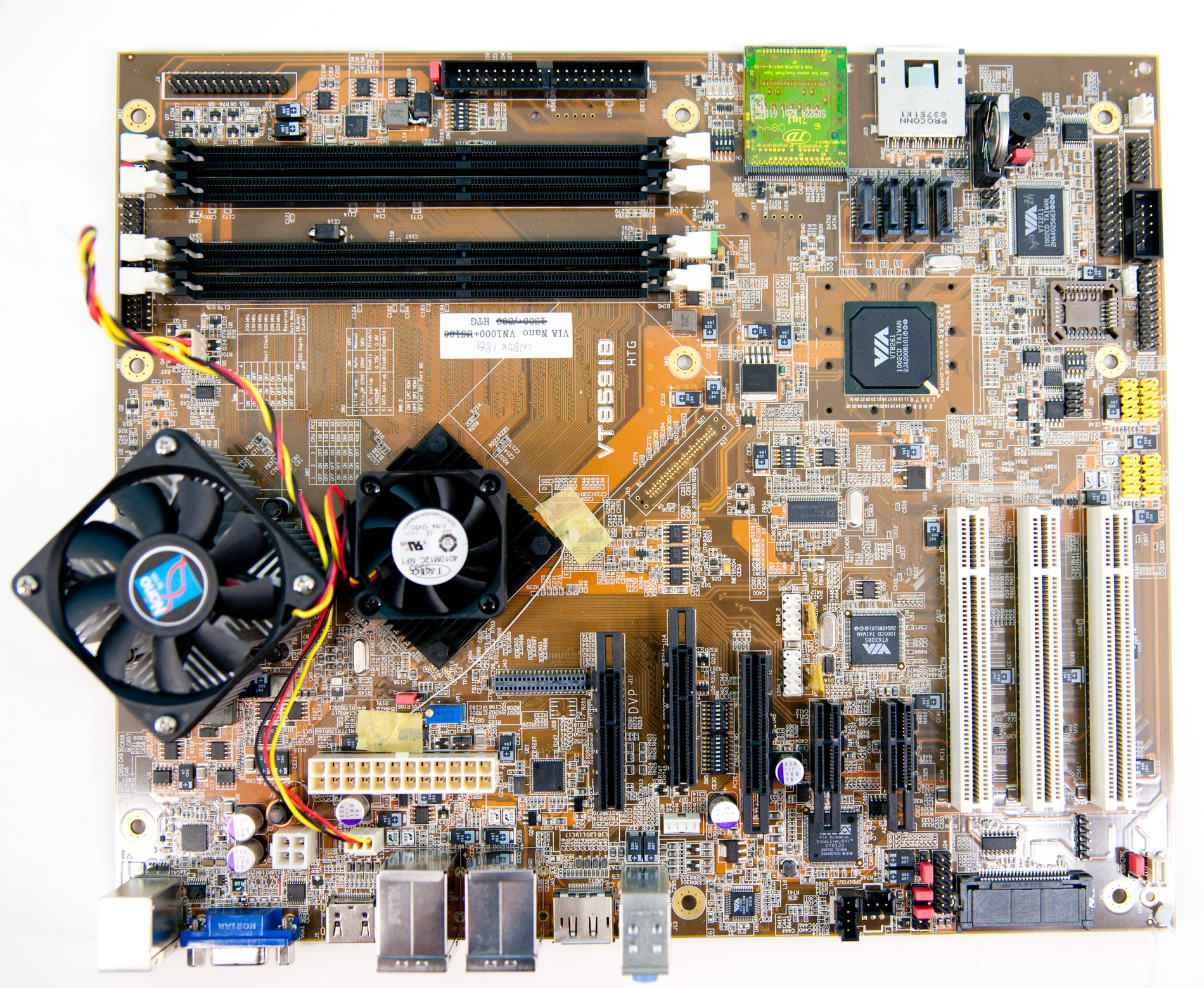
Armed with a reference ATX motherboard, I was eager to verify those claims. Note that this review appears a lot later than expected as our original DC Nano reference board was damaged in transport. It wouldn't do anything beyond POST so what you're looking at is our second sample.


54 Comments
View All Comments
tipoo - Monday, November 15, 2010 - link
So what I take from this is that performance usually beats Atom+Intel IGP, but that 65nm fabrication process means they aren't competitive in power draw.IntelUser2000 - Monday, November 15, 2010 - link
Sorry, AMD on the same 40nm TSMC will have similar performance for CPU, and have far less TDP.No, Via's designs are just years and years behind. They probably need 22nm RIGHT NOW to be competitive.
tipoo - Monday, November 15, 2010 - link
Huh? This is 65nm, and like you yourself said AMD's is on 40nm. Its not the same like you said. But you are right in saying that it also needs architectural improvements.DanNeely - Monday, November 15, 2010 - link
40nm will help a lot on load power, but until they implement power gating (and this is somewhere Intel still leads AMD significantly) idle power is going to remain a major liability.chucky2 - Monday, November 15, 2010 - link
Forget the speed of this thing for a moment, and the power consumption:What about stability and compatibility?
If VIA is going to try and make a come back - of any type - then reviewers need to do much more stability and compatibilty testing than with products based on Intel or AMD solutions, as those were the major issues with VIA in the past. It wasn't that they had bad speed or high power consumption of the money you paid for them, it's that they had an unacceptable level of stability and compatibility issues.
For anyone familiar with the VIA of old, that will be the benchmark they're weighed against before speed or power consumption even come into question. Doesn't matter how fast something is, or how little power it consumes, if there's a good chance it's going to crash on me with regular usage, or, if the common component I'll be plugging into it is going to have issues (because of VIA) or crash (because of VIA).
Sure hope VIA learned from its past history.......
Chuck
strikeback03 - Monday, November 15, 2010 - link
Well this is labeled as a preview, maybe more of that will come when they have final shipping hardware.ProDigit - Monday, November 15, 2010 - link
Please, when you review bobcat, compare it to this nano chip!The results might prove interesting.
I believe the Nano could have better CPU, while worse GPU ratings than the AMD one.
Power consumption of the Nano @40nm should be between 28W and 40W idle/load; unless they are able to optimize the nano, and integrate some overclocking (like intel's turbo boost technology).
It'd be nice to see some downclocking or core disablement on this cpu too!
Via has much to invest in if it wants to be competitive with Intel!
nitrousoxide - Monday, November 15, 2010 - link
It will not out-perform Fusion APU, which has approximately 80% the performance of current low-voltage Athlon II X2 CPUs, that is really impressive power.Zingam - Monday, November 15, 2010 - link
nvidia should buy themShloader - Monday, November 15, 2010 - link
Actually... Yeah! If not that then at the very least create a strong partnership with them. Were that to happen a lot of the Linux compatibility questions go right out the window (unfortunately letting in a lot of power consumption questions). nVidia needs to team up with a player in the x86 CPU market and insure a platform for their discreet graphics + chipset business. Remember it was nVidia that led the way to dual channel memory on the x86 platform. Get that DDR3 memory controller integrated along with an integrated nVidia GPU on a 22 to 32 nm process. I would actually buy something for HTPC if both those companies shared the helm. nVidia's additions would make a lot of the core performance questions irrelevant for me. Just give me enough cuda power to play my vids while speeding up h.264 encoding.