NVIDIA's GeForce GTX 580: Fermi Refined
by Ryan Smith on November 9, 2010 9:00 AM ESTThe GTX 480… it’s hotter, it’s noisier, and it’s more power hungry, all for 10-15% more performance. If you need the fastest thing you can get then the choice is clear, otherwise you’ll have some thinking to decide what you want and what you’re willing to live with in return.
The GeForce GTX 480 and the associated GF100 GPU have presented us with an interesting situation over the last year. On the one hand NVIDIA reclaimed their crown for the fastest single GPU card on the market, and in time used the same GPU to give rise to a new breed of HPC cards that have significantly expanded the capabilities of GPU computing. On the other hand, like a worn and weary athlete finally crossing the finish line, this didn’t come easy for NVIDIA. GF100 was late, and the GTX 480 while fast was still hot & loud for what it was.
Furthermore GTX 480 and GF100 were clearly not the products that NVIDIA first envisioned. We never saw a product using GF100 ship with all of its SMs enabled – the consumer space topped out at 15 of 16 SMs, and in the HPC space Tesla was only available with 14 of 16 SMs. Meanwhile GF100’s younger, punchier siblings put up quite a fight in the consumer space, and while they never were a threat to GF100, it ended up being quite the surprise for how close they came.
Ultimately the Fermi architecture at the heart of this generation is solid – NVIDIA had to make some tradeoffs to get a good gaming GPU and a good compute GPU in a single product, but it worked out. The same can’t be said for GF100, as its large size coupled with TSMC’s still-maturing 40nm process lead to an unwieldy combination that produced flakey yields and leaky transistors. Regardless of who’s ultimately to blame, GF100 was not the chip it was meant to be.
But time heals all wounds. With GF100 out the door NVIDIA has had a chance to examine their design, and TSMC the chance to work the last kinks out of their 40nm process. GF100 was the first Fermi chip, and it would not be the last. With a lesson in hand and a plan in mind, NVIDIA went back to the drawing board to fix and enhance GF100. The end result: GF110, the next iteration of Fermi. Hot out of the oven, it is launching first in the consumer space and is forming the backbone of the first card in NVIDIA’s next GeForce series: GeForce 500. Launching today is the first such card, the GF110-powered GeForce GTX 580.
| GTX 580 | GTX 480 | GTX 460 1GB | GTX 285 | |
| Stream Processors | 512 | 480 | 336 | 240 |
| Texture Address / Filtering | 64/64 | 60/60 | 56/56 | 80 / 80 |
| ROPs | 48 | 48 | 32 | 32 |
| Core Clock | 772MHz | 700MHz | 675MHz | 648MHz |
| Shader Clock | 1544MHz | 1401MHz | 1350MHz | 1476MHz |
| Memory Clock | 1002MHz (4008MHz data rate) GDDR5 | 924MHz (3696MHz data rate) GDDR5 | 900Mhz (3.6GHz data rate) GDDR5 | 1242MHz (2484MHz data rate) GDDR3 |
| Memory Bus Width | 384-bit | 384-bit | 256-bit | 512-bit |
| Frame Buffer | 1.5GB | 1.5GB | 1GB | 1GB |
| FP64 | 1/8 FP32 | 1/8 FP32 | 1/12 FP32 | 1/12 FP32 |
| Transistor Count | 3B | 3B | 1.95B | 1.4B |
| Manufacturing Process | TSMC 40nm | TSMC 40nm | TSMC 40nm | TSMC 55nm |
| Price Point | $499 | ~$420 | ~$190 | N/A |
GF110 is a mix of old and new. To call it a brand-new design would be disingenuous, but to call it a fixed GF100 would be equally shortsighted. GF110 does have a lot in common with GF100, but as we’ll see when we get in to the design of GF110 it is its own GPU. In terms of physical attributes it’s very close to GF100; the transistor count remains at 3 billion (with NVIDIA undoubtedly taking advantage of the low precision of that number), while the die size is at 520mm2. NVIDIA never did give us the die size for GF100, but commonly accepted values put it at around 530mm2, meaning GF110 is a hair smaller.
But before we get too deep in to GF110, let’s start with today’s launch card, the GeForce GTX 580. GTX 580 is the first member of the GeForce 500 series, giving it the distinction of setting precedent for the rest of the family that NVIDIA claims will soon follow. Much like AMD last month, NVIDIA is on their second trip with the 40nm process, meaning they’ve had the chance to refine their techniques but not the opportunity to significantly overhaul their designs. As a result the 500 series is going to be very familiar to the 400 series – there really aren’t any surprises or miracle features to talk about. So in many senses, what we’re looking at today is a faster version of the GTX 480.
So what makes GTX 580 faster? We’ll start with the obvious: it’s a complete chip. All the L2 cache, all the ROPs, all the SMs, it’s all enabled. When it comes to gaming this is as fast as GF110 can be, and it’s only through NVIDIA’s artificial FP64 limitations that double-precision computing isn’t equally unrestricted. We have wondered for quite some time what a full GF100 chip would perform like – given that GTX 480 was short on texture units, shaders, and polymorph engines, but not ROPs – and now the answer is at hand. From all of this GTX 580 has 6.6% more shading, texturing, and geometric performance than the GTX 480 at the same clockspeeds. Meanwhile the ROP count and L2 cache remains unchanged; 48 ROPs are attached to 768KB L2 cache, which in turn are attached to 6 64bit memory controllers.
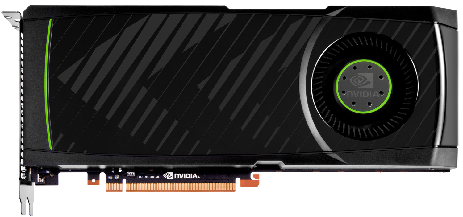
GeForce GTX 580
The second change of course is clockspeeds. The reference GTX 480 design ran at 700MHz for the core and 924MHz (3696MHz data rate) for the GDDR5. Meanwhile GTX 580 brings that up to 772MHz for the core and 1002MHz (4008MHz data rate), marking a 72MHz(10%) increase in core clockspeed and a slightly more modest 78MHz (8%) increase in memory bandwidth. This is a near-equal increase in the amount of work that GTX 580 can process and the amount of work its memory can feed it, which should offer a relatively straightforward increase in performance.
Last but certainly not least change coming from GTX 480 is in GF110 itself. NViDIA has ported over GF104’s faster FP16 (half-precision) texture filtering capabilities, giving GF110/GTX580 the ability to filter 4 FP16 pixels per clock, versus 2 on GF100/GTX480. The other change ties in well with the company’s heavy focus on tessellation, with a revised Z-culling/rejection engine that will do a better job of throwing out pixels early, giving GF110/GTX580 more time to spend on rendering the pixels that will actually be seen. This is harder to quantify (and impossible for us to test), but NVIDIA puts this at another 8% performance improvement.
Meanwhile NVIDIA hasn’t ignored GTX 480’s hot and loud history, and has spent some time working on things from that angle. We’ll dive in to NVIDIA’s specific changes later, but the end result is that through some optimization work they’ve managed to reduce their official TDP from 250W on the GTX 480 to 244W on the GTX 580, and in practice the difference is greater than that. NVIDIA’s cooling system of choice has also been updated, working in tandem with GTX 580’s lower power consumption to bring down temperatures and noises. The end result is a card that should be and is cooler and quieter while at the same being faster than GTX 480.
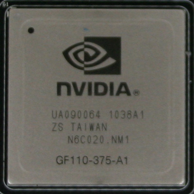
GF110
The downside to this is that if it sounds like a fairy tale, it almost is. As you’ll see we have a rather high opinion of GTX 580, but we’re not convinced you’re going to be able to get one quite yet. NVIDIA is technically hard-launching GTX 580 today at $499 (GTX 480’s old price point), but they aren’t being very talkative about the launch quantity. They claim it’s for competitive reasons (to keep AMD from finding out) and we can certainly respect that, but at the same time it’s rare in this industry for someone to withhold information because it’s a good thing. We really hope to be surprised today and see GTX 580s available for everyone that wants one, but we strongly suspect that it’s going to be available in low quantities and will sell out very quickly. After that it’s anyone’s guess on what the refresh supply will be like; our impression of matters is that yields are reasonable for such a large chip, but that NVIDIA didn’t spend a lot of time stockpiling for today’s launch.
In any case, with GTX 580 taking the $500 spot and GF110 ultimately destined to replace GF100, GF100 based cards are going to be on their way out. NVIDIA doesn’t have an official timeline, but we can’t imagine they’ll continue producing GF100 GPUs any longer than necessary. As a result the GTX 480 and GTX 470 are priced to go, falling between the GTX 580 and the GTX 460 in NVIDIA’s lineup for now until they’re ultimately replaced with other 500 series parts. For the time being this puts the GTX 480 at around $400-$420, and the GTX 470 – still doing battle with the Radeon HD 6870 – is at $239-$259.
Meanwhile AMD does not have a direct competitor for the GTX 580 at the moment, so their closest competition is going to be multi-GPU configurations. In the single card space there’s the Radeon HD 5970, which is destined for replacement soon and as a result AMD is doing what they can to sell off Cypress GPUs by the end of the year. The last reference 5970 you can find on Newegg is a Sapphire card, which is quite blatantly priced against the GTX 580 at $499 with a $30 rebate. Given that it’s the last 5970, we’d be surprised if it was in stock for much longer than the initial GTX 580 shipments.
For cards you do stand a good chance of getting, a pair of 6870s will set you back between $480 and $500, making it a straightforward competitor to the GTX 580 in terms of price. A pair of cards isn’t the best competitor, but CrossFire support is widely available on motherboards so it’s a practical solution at that price.
| Fall 2010 Video Card MSRPs | ||
| NVIDIA | Price | AMD |
|
GeForce GTX 580
|
$500 | Radeon HD 5970 |
| $420 | ||
|
|
$300 | Radeon HD 5870 |
| $240 | Radeon HD 6870 | |
| $180 | Radeon HD 6850 | |


160 Comments
View All Comments
cjb110 - Tuesday, November 9, 2010 - link
"The thermal pads connecting the memory to the shroud have once again wiped out the chip markets", wow powerful adhesive that! Bet Intel's pissed.cjb110 - Tuesday, November 9, 2010 - link
"While the difference is’ earthshattering, it’s big enough..." nt got dropped, though not yet at my workplace:)Invader Mig - Tuesday, November 9, 2010 - link
I don't know the stance on posting links to other reviews since I'm a new poster, so I wont. I would like to make note that in another review they claim to have found a work around the power throttling that allowed them to use furmark to get accurate temps and power readings. This review has the 580 at 28w above the 480 at max load. I don't mean to step on anyone's toe's, but I have seen so many different numbers because of this garbage nvidia has pulled, and the only person who claims to have furmark working gets higher numbers. I would really like to see something definitive.7Enigma - Tuesday, November 9, 2010 - link
Here's my conundrum. What is the point of something like Furmark that has no purpose except to overstress a product? In this case the 580 (with modified X program) doesn't explode and remains within some set thermal envelope that is safe to the card. I like using Crysis as it's a real-world application that stresses the GPU heavily.Until we have another game/program that is used routinely (be it game or coding) that surpasses the heat generation and power draw of Crysis I just don't see the need to try to max out the cards with a benchmark. OC your card to the ends of the earth and run something real, that is understandable. But just using a program that has no real use to artificially create a power draw just doesn't have any benefit IMO.
Gonemad - Tuesday, November 9, 2010 - link
I beg to differ. (be careful, high doses of flaming.)Let me put it like this. The Abrams M1 Tank is tested on a 60º ramp (yes, that is sixty degrees), where it must park. Just park there, hold the brakes, and then let go. It proves the brakes on a 120-ton 1200hp vehicle will work. It is also tested on emergency brakes, where this sucker can pull a full stop from 50mph on 3 rubber-burning meters. (The treads have rubber pads, for the ill informed).
Will ever a tank need to hold on a 60º ramp? Probably not. Would it ever need to come to a screeching halt in 3 meters? In Iraqi, they probably did, in order to avoid IEDs. But you know, if there were no prior testing, nobody would know.
I think there should be programs specifically designed to stress the GPU in unintended ways, and it must protect itself from destruction, regardless of what code is being thrown at it. NVIDIA should be grateful somebody pointed that out to them. AMD was thankful when they found out the 5800 series GPUs (and others, but this was worse) had lousy performance on 2D acceleration, or none at all, and rushed to fix its drivers. Instead, NVIDIA tries to cheat Furmark by recognizing its code and throttling. Pathetic.
Perhaps someday, a scientific application may come up with repeatable math operations that just behave exactly like Furmark. So, out of the blue, you got a $500 worth of equipment that gets burned out, and nobody can tell why??? Would you like that happening to you? Wouldn't you like to be informed that this or that code, at least, could destroy your equipment?
What if Furmark wasn't designed to stress GPUs, but it was an actual game, (with furry creatures, lol)?
Ever heard of Final Fantasy XIII killing off PS3s for good, due to overload, thermal runaway, followed by meltdown? Rumors are there, if you believe them is entirely to you.
Ever heard of Nissan GTR (skyline) being released with a top-speed limiter with GPS that unlocks itself when the car enters the premises of Nissan-approved racetracks? Inherent safety, or meddling? Can't you drive on a Autoban at 300km/h?
Remember back in the day of early benchmark tools, (3DMark 2001 if I am not mistaken), where the Geforce drivers detected the 3DMark executable and cheated the hell out of the results, and some reviewers got NVIDIA red-handed when they renamed and changed the checksum of the benchmark??? Rumors, rumors...
The point is, if there is a flaw, a risk of an unintended instruction kill the hardware, the buyer should be rightfully informed of such conditions, specially if the company has no intention at all to fix it. Since Anand warned us, they will probably release the GTX 585 with full hardware thermal safeties. Or new drivers. Or not.
Just like the instruction #PROCHOT was inserted in the Pentium (which version?) and some reviewers tested it against an AMD chip. I never forgot that AMD processor billowing blue smoke the moment the heatsink was torn off. Good PR, bad PR. The video didn´t look fake to me back then, just unfair.
In the end, it becomes matter of PR. If suddenly all the people that played Crysis on this card caused it to be torched, we would have something really interesting.
Sihastru - Tuesday, November 9, 2010 - link
AMD has a similar system in place since the HD4xx0 generation. Remember when Furmark used to blow up 48x0 cards? Of course not. But look it up...What nVidia did here is what AMD has in all their mid/high end cards since HD4xx0. At least nVidia will only throttle when it detects Furmark/OCCT. AMD cards will throttle in any situation if the power limiter requires it.
JimmiG - Tuesday, November 9, 2010 - link
It's a very unfortunate situation that both companies are to blame for. That's what happens when you push the limits of power consumption and heat output too far while at the same time trying to keep manufacturing costs down.The point of a stress test is to push the system to the very limit (but *not* beyond it, like AMD and Nvidia would have you believe). You can then be 100% assured that it will run all current and future games and HPC applications, not matter what unusual workloads they dump on your GPU or CPU, without crashes or reduced performance.
cactusdog - Tuesday, November 9, 2010 - link
So if you want to use multiple monitors do you still need 2 cards to run it or have they enabled a third monitor on the 580?Sihastru - Tuesday, November 9, 2010 - link
Yes.Haydyn323 - Tuesday, November 9, 2010 - link
The 580 as with the previous generation still only supports 2 monitors max per card.