GTC 2010 Day 1: NVIDIA Announces Future GPU Families for 2011 And 2013
by Ryan Smith on September 22, 2010 2:46 AM ESTAs we mentioned last week, we’re currently down in San Jose, California covering NVIDIA’s annual GPU Technology Conference. If Intel has IDF and Apple has the World Wide Developers Conference, then GTC is NVIDIA’s annual powwow to rally their developers and discuss their forthcoming plans. The comparison to WWDC is particularly apt, as GTC is a professional conference focused on development and business use of the compute capabilities of NVIDIA’s GPUs (e.g. the Tesla market).
NVIDIA has been pushing GPUs as computing devices for a few years now, as they see it as the next avenue of significant growth for the company. GTC is fairly young – the show emerged from NVISION and its first official year was just last year – but it’s clear that NVIDIA’s GPU compute efforts are gaining steam. The number of talks and the number of vendors at GTC is up compared to last year, and according to NVIDIA’s numbers, so is the number of registered developers.

We’ll be here for the next two days meeting with NVIDIA and other companies and checking out the show floor. Much of this trip is to get a better grasp on just where things are for NVIDIA still-fledging GPU compute efforts, especially on the consumer front where GPU compute usage has been much flatter than we were hoping for at this time last year with the announcement/release of NVIDIA and AMD’s next-generation GPUs, and the ancillary launch of APIs such as DirectCompute and OpenCL, which are intended to allow developers to write an application against these common APIs rather than targeting CUDA or Brook+/Stream. If nothing else, we’re hoping to see where our own efforts in covering GPU computing need to lie – we want to add more compute tests to our GPU benchmarks, but is the market to the point yet where there’s going to be significant GPU compute usage in consumer applications? This is what we’ll be finding out over the next two days.
Jen-Hsun Huang Announces NVIDIA’s Next Two GPUs
While we’re only going to be on the show floor Wednesday and Thursday, GTC unofficially kicked off Monday, and the first official day of the show was Tuesday. Tuesday started off with a 2 hour keynote speech by NVIDIA’s CEO Jen-Hsun Huang, which keeping with the theme of GTC focused on the use of NVIDIA GPUs in business environments.
Not unlike GTC 2009, NVIDIA is also using the show as a chance to announce their next-generation GPUs. GTC 2009 saw the announcement of the Fermi family, with NVIDIA first releasing the details of the GPU’s compute capabilities there, before moving on to focusing on gaming at CES 2010. This year NVIDIA announced the next two GPU families the company is working on, albeit not in as much detail as we got about Fermi in 2009.
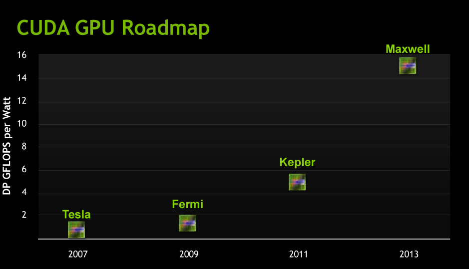
The progression of NVIDIA's GPUs from a Tesla/Compute Standpoint
The first GPU is called Kepler (as in Johannes Kepler the mathematician), which will be released in the 2nd half of 2011. At this point the GPU is still a good year out, which is why NVIDIA is not talking about its details just yet. For now they’re merely talking about performance in an abstract manner, in this case Kepler should offer 3-4 times the amount of double precision floating point performance per watt of Fermi. With GF100 NVIDIA basically hit the wall for power consumption (and this is part of the reason current Tesla parts are running 448 out of 512 CUDA cores), so we’re basically looking at NVIDIA having to earn their performance improvements without increasing power consumption. They’re also going to have to earn their keep in sales, as NVIDIA is already talking about Kepler taking 2 billion dollars to develop and it’s not out for another year.
The second GPU is Maxwell (named after James Clerk Maxwell, the physicist/mathematician), and will be released some time in 2013. Compared to Fermi it should offer 10-12 times the DP FP performance per watt, which means it’s roughly another 3x increase over Kepler.
![]()
NVIDIA GPUs and manufacturing processes up to Fermi
NVIDIA still has to release the finer details of the GPUs, but we do know that Kepler and Maxwell are tied to the 28nm and 22nm processes respectively. So if nothing else, this gives us strong guidance on when they would be coming out, as production-quality 28nm fabrication suitable for GPUs is still a year out and 22nm is probably a late 2013 release at this rate. What’s clear is that NVIDIA is not going to take a tick-tock approach as stringently as Intel did – Kepler and Maxwell are going to launch against new processes – but this is only about GPUs for NVIDIA’s compute efforts. It’s likely the company will still emulate tick-tock to some degree, producing old architectures on new processes first; similar to how NVIDIA’s first 40nm products were the GT21x GPUs. In this scenario we’re talking about low-end GPUs destined for life in consumer video cards, so the desktop/graphics side of NVIDIA isn’t bound to this schedule like the Fermi/compute side is.
At this point the biggest question is going to be what the architecture is. NVIDIA has invested heavily in their current architecture ever since the G80 days, and even Fermi built upon that. It’s a safe bet that these next two GPUs are going to maintain the same (super)scalar design for the CUDA cores, but beyond that anything is possible. This also doesn’t say anything about what the GPUs’ performance is going to be like under single precision floating point or gaming. If NVIDIA focuses almost exclusively on DP, we could see GPUs that are significantly faster at that while not being much better at anything else. Conversely they could build more of everything and these GPUs would be 3-4 times faster at more than just DP.
Gaming of course is a whole other can of worms. NVIDIA certainly hasn’t forgotten about gaming, but GTC is not the place for it. Whatever the gaming capabilities of these GPUs are, we won’t know for quite a while. After all, NVIDIA still hasn’t launched GF108 for the low-end.
Wrapping things up, don’t be surprised if Kepler details continue to trickle out over the next year. NVIDIA took some criticism for introducing Fermi months before it shipped, but it seems to have worked out well for the company anyhow. So a repeat performance wouldn’t be all that uncharacteristic for them.
And on that note, we’re out of here. We’ll have more tomorrow from the GTC show floor.


82 Comments
View All Comments
AlexWade - Wednesday, September 22, 2010 - link
Wikipedia has some entries about the new AMD HD6xxx series. I don't know how true it is, but some of the dates are not too far away. This may or may not help you.http://en.wikipedia.org/wiki/Comparison_of_AMD_gra...
If the estimates are mostly true, the HD6xxx series looks like it will be really good. The GFLOPS of the HD5870 is 2070 according the wikipedia page, and 4080 for the HD6870. That is almost double the performance for 40W more. It looks like no DirectX 12 either.
Dark_Archonis - Wednesday, September 22, 2010 - link
It was way too early for anyone to be releasing DirectX 12 cards. Such cards won't be out for a long while, and Microsoft won't even be releasing DirectX 12 for a while either. The current information shows that Microsoft won't release DirectX 12 until mid-2012 at the earliest.Lanskuat - Wednesday, September 22, 2010 - link
NVidia had big problems with big GF100 chip, so I think they make now a small chip like GF106 and AMD RV870, at this case it will be not 2x times large in transistor count, but something 1.5x large. So Kepler high end card on 28 nm will be with ~ 768 CUDA cores and raised frequirences. They don't need to make new architecture, because GTX 480 SLI with 960 CUDAs works very well. I think everybody wanted to have such single card.Dark_Archonis - Wednesday, September 22, 2010 - link
Nvidia could rework current Fermi cards to get better efficiency and performance, just like they did when the reworked the GTX 480 design to the GTX 460 design.Nvidia could potentially add more shader and texture units for the same number of CUDA cores, and improve their memory controller to achieve better performance and efficiency without increasing die size that much. Nvidia could also add an additional warp scheduler to the GF104 design to improve efficiency and performance without much die size increase.
Fermi is a modular architecture which gives Nvidia some flexibility in making variations or improved versions of Fermi cards.
Touche - Wednesday, September 22, 2010 - link
Lots of coulds in that one.Will Robinson - Wednesday, September 22, 2010 - link
It's still trying to put lipstick on a pig.No wonder NVDA has fallen to the level of 2nd tier graphics chip maker now.
JeffC. - Wednesday, September 22, 2010 - link
I would argue that Nvidia has a different approach to the graphics industry and is more beneficial to professionals in the field. AMD does not position their graphics division to cater to professionals the same as Nvidia. If nV’s revenue did not rely on consumer graphics cards so much, they could leave the market and still be a big player in the graphics industry. However, many gamers who do not read extensively in the tech industry form their opinions based only on consumer level graphics cards; that’s not saying *AMD’s current line-up is better in all ways measurable. IMO, AMD’s focus for their graphics division and formerly ATI’s position is engineering graphics cards specifically for the consumer level market. Nvidia may need to completely separate their teams for consumer graphics cards and professional graphics cards instead of leveraging Tesla to subsidize the rest of the architecture. That way we would have cards engineered specifically for consumers and professionals.fteoath64 - Thursday, September 23, 2010 - link
I would not think the Tesla is subsidizing the consumer cards. The NV approach makes sense in leveraging the maximum resources (people) to create multiple product of similar capabilities but doing it from 'Big to small" rather than ground up. The high risk is the Big Product needs to be done quickly so the variations can be harvested/tweaked allowing for the needed diversity of the market. Having separate teams will reduce the software throughput of the drivers and associated platforms it targets.JeffC. - Thursday, September 23, 2010 - link
I'm sure the Tesla line leads in margin compared to the rest of their products. This allows some freedom in pricing with regards to Geforce. The focus of the different markets is getting to the point where it's affecting the efficiency of mainly their high-end consumer cards.If they separated things more, the basic architecture could still be the same and thus the software not much different. Furthermore, die space is allocated for things that the consumer space is not using at the moment. There are different approaches. Nvidia's approach is not really allowing them to be as competitive as they could be with Geforce.Dark_Archonis - Thursday, September 23, 2010 - link
Well the more of these comments I see, the more I begin to wonder how many posters here work for ATI's PR department.Nvidia, "2nd tier" graphics maker? You sir have no idea what you are talking about.
I would highly encourage you to stop posting such nonsense and look up the new Quadro cards and how they obliterate comparable FirePro cards in the professional graphics market.
There is more to the graphics market than just gaming.