Intel's Sandy Bridge Architecture Exposed
by Anand Lal Shimpi on September 14, 2010 4:10 AM EST- Posted in
- CPUs
- Intel
- Sandy Bridge
The Ring Bus
With Nehalem/Westmere all cores, whether dual, quad or six of them, had their own private path to the last level (L3) cache. That’s roughly 1000 wires per core. The problem with this approach is that it doesn’t work well as you scale up in things that need access to the L3 cache.
Sandy Bridge adds a GPU and video transcoding engine on-die that share the L3 cache. Rather than laying out another 2000 wires to the L3 cache Intel introduced a ring bus.
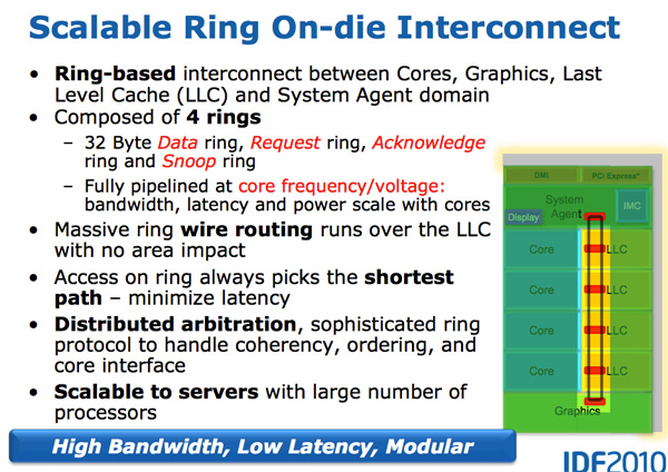
Architecturally, this is the same ring bus used in Nehalem EX and Westmere EX. Each core, each slice of L3 (LLC) cache, the on-die GPU, media engine and the system agent (fancy word for North Bridge) all have a stop on the ring bus.
The bus is made up of four independent rings: a data ring, request ring, acknowledge ring and snoop ring. Each stop for each ring can accept 32-bytes of data per clock. As you increase core count and cache size, your cache bandwidth increases accordingly.
Per core you get the same amount of L3 cache bandwidth as in high end Westmere parts - 96GB/s. Aggregate bandwidth is 4x that in a quad-core system since you get a ring stop per core (384GB/s).
L3 latency is significantly reduced from around 36 cycles in Westmere to 26 - 31 cycles in Sandy Bridge. We saw this in our Sandy Bridge preview and now have absolute numbers in hand. The variable cache latency has to do with what core is accessing what slice of cache.
Also unlike Westmere, the L3 cache now runs at the core clock speed - the concept of the un-core still exists but Intel calls it the “system agent” instead and it no longer includes the L3 cache.
With the L3 cache running at the core clock you get the benefit of a much faster cache. The downside is the L3 underclocks itself in tandem with the processor cores. If the GPU needs the L3 while the CPUs are downclocked, the L3 cache won’t be running as fast as it could had it been independent.
The L3 cache is divided into slices, one associated with each core although each core can address the entire cache. Each slice gets its own stop and each slice has a full cache pipeline. In Westmere there was a single cache pipeline and queue that all cores forwarded requests to, in Sandy Bridge it’s distributed per cache slice.
The ring wire routing runs entirely over the L3 cache with no die area impact. This is particularly important as you effectively get more cache bandwidth without any increase in die area. It also allows Intel to scale the core count and cache size without incurring additional ring-related die area.
Each of the consumers/producers on the ring get their own stop. The ring always takes the shortest path. Bus arbitration is distributed on the ring, each stop knows if there’s an empty slot on the ring one clock before.
The System Agent
For some reason Intel stopped using the term un-core, instead in Sandy Bridge it’s called the System Agent.
The System Agent houses the traditional North Bridge. You get a 16 PCIe 2.0 lanes that can be split into two x8s. There’s a redesigned dual-channel DDR3 memory controller that finally restores memory latency to around Lynnfield levels (Clarkdale moved the memory controller off the CPU die and onto the GPU).
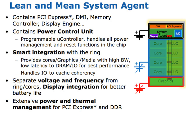
The SA also has the DMI interface, display engine and the PCU (Power Control Unit). The SA clock speed is lower than the rest of the core and it is on its own power plane.


62 Comments
View All Comments
JoJoman88 - Wednesday, September 15, 2010 - link
To me the problem is that instead of me overclocking without reguard to TDP, now Intel will do the overclocking for me, but it will be within the TDP that Intel thinks is best. Will this not just kill the after-market cooler makers with an almost locked TDP,and to some degree high end memory maker with a locked BCLK.This will change how overclocking is done from now on unless AMD keeps things as they are and forces Intel from going down this road.
gvaley - Wednesday, September 15, 2010 - link
It's true that the CPU will turboboost within the CPU's TDP, but exactly how much it will turboboost (how much bins it will gain) will depend on how well the CPU is being chilled. So having a better (read: aftermarket) cooler will allow you to take the best of your CPU's turboboost.shodanshok - Wednesday, September 15, 2010 - link
Hi Anand,while I expect the ring bus to provide great performances, I doubt that it don't impact die size and power consumption in respect to the Nehalem/Westmere L3 organization.
Let me explain...
From my internal test, the Nehalem/Westmere L3 cache seems accessed by a four 64 bit channels (one per core). At 3 Ghz L3 cache, it translate in a maximum of 24 GB/s per core, or 96 GB/s for 4 cores. This cache organization seems confirmed by the tests at Techreport (on a i975X, SANDRA's L3 cumulative bandwidth is at about 60 GB/s: http://www.techreport.com/articles.x/18581/5) and Xbitlabs (EVEREST single-core L3 bandwidth of about 20 GB/s: http://www.xbitlabs.com/articles/cpu/display/intel...
So, on Nehalem/Westmere I do not expect 4 x 256 wires, but only 4 x 64 wires (more or less).
Now, lets examine SB...
We have 4 x 256 bit bus (4 indipendent rings) that runs around the L3 cache, for a total of 1024 wires. So, we have a lot of wires, that needs to be powered. These wires, in turn, need additional die space, and to me seems the main reason why most models will have "only" a 6 MB L3.
What do you think about? It is possible to ask Intel something about the Nehalem L3 cache organization and/or about the decision to equip most SB models with 6 MB of L3 cache?
Thanks.
Casper42 - Wednesday, September 15, 2010 - link
Knowing what you do about Nehalem EX and SNB on socket H2, any speculation on what we can expect from the Socket B2/R chips when they finally arrive sometime next year?I am mainly thinking of Northbridge/QPI and PCIe Lanes as compared to DMI used on the Mainstream parts discussed in this article.
I waited and waited for Westmere Core i7 to become "cheap" and thought the 970 was going to be my chip of choice @ $550. When they released it at $900 (you could already find 980Xs for less) it pretty much killed my plans to upgrade.
So now I am basically debating on do I build a high end H2 or wait for the enthusiast version to arrive instead?
My understanding from seeing the server roadmap is there will be Socket B2 and Socket R with the differences between them mainly consisting of memory channels and # of PCIe Lanes. I have also read that both will support PCIe 3.0 whereas H2 will continue to use 2.0.
Add all these changes up and I am also hopeful we will see USB3 on the Enthusiast platform as well since it will have an additional 3-6 months to mature.
So any ideas/insight you have here would be awesome.
linkages - Thursday, September 16, 2010 - link
With the price of LCDs dropping, I am noticing that more and more consumers have more than one display for their mainstream machines. Has Intel said anything about how many displays the onboard graphics will be able to push? Have they said anything about what tech they are going to use ie. display port, HDMI, DVI-D, something else?I can see myself getting a new SB machine sometime in Q1 2011 but I run at least 2 monitors at all times ( need the real estate for the type of work that I do ). I don't play many games but having the video decode/encode is important to me since I do tend to do some videoconferencing now a days.
The last thing I would like to know is if Intel is going to do the right thing with the drivers for their graphics. Will we humble linux users finally have a graphics driver that does not suck. Will Intel finally open source the driver so that the community can keep it updated and optimize it for X?
chukked - Thursday, September 16, 2010 - link
Hi Anand,thanks for the review, you addressed everything but left virtualization :(
which processors support vt-x and vt-d ?
iwodo - Friday, September 17, 2010 - link
x264, the best h.264 encoder there is, produce better quality video and similar speed when using "ultrafast" setting. And with 2 / 4 Core we could even transcode 2 - 4 video at the same time.The hardware encoder inside SandyBridge is not that speedy. While i could scarifies quality for speed. But Power VR's VRE Core manage 1000fps +, @ 400fps the encoder is like a waste of die space.
Intel could have further tuned the x264 for Sandy Bridge for speed and just release it with their drivers. If the hardware encoder aren't giving many times the increase in speed, then what is the point? They may as well have added extra 6 EU for GPU inside.
A Link to someone's blog posting some figures.
http://lee.hdgreetings.com/2010/09/intel-cpu-vs-nv...
Wolfpup - Wednesday, September 29, 2010 - link
Pretty disappointing. I'm sure AMD's glad though!10-30% improvement-obviously that's great, but not as big as their previous tocks if I'm remembering right, and not much different from what "ticks" like Penryn did...I know Penryn was like a 10% boost minimum over Conroe...
I'm guessing it's because they're wasting effort and die area on a worthless GPU. I *HOPE* no one on this site, no power users are going to be using that thing. (Well, okay, for a tiny notebook or something maybe...)
JumpingJack - Wednesday, September 29, 2010 - link
I don't believe you are remembering correctly.Conroe was the first tock, and certainly, it was a major leap over the P4 line. But it's bloodline was actually derived from P6, which was carried through from Banias, Dothan, then Yohna. The improvement over Yohna was in the 10-20% IPC range.
Then came Penryn the tick, which was on average only 5%, http://www.anandtech.com/show/2306/3
Then came the tock, which was Nehalem. In single threaded performance, it was roughly another 5-10% over Penryn, but in multithreaded -- again, clock for clock, it had leaps of performance, around 20-40% again. http://www.anandtech.com/show/2658/20
The tick of Nehalem was Westmere, now Westmere did not launch a quad core part so it is hard to find a clock for clock, but in single threaded performance -- roughly the same as Nehalem, factoring out any turbo advantages...
Now SB, a tick, with another 10-30% across the board both single and multithreaded, depending on workload.
Of course, the GPU is not so worthless, it is indeed challenging low end GPUs -- no doubt Llano will offer up strong GPU performance, but for the majority of the market SB is perfectly fine.
Indeed, AMD is not too happy here, at least I would suspect. On the CPU side, Intel will crush anything AMD has in the same market segement where SB resides... GPU, surely AMD will crush SB. On the CPU front, AMD is already 20-40% behind Nehalem clock for clock, core for core, SB just extends that another 10-30%.
gundersausage - Tuesday, October 26, 2010 - link
i7-950 vs i7-2500K... So which will be faster and a better gaming chip? anyone?