Intel's Sandy Bridge Architecture Exposed
by Anand Lal Shimpi on September 14, 2010 4:10 AM EST- Posted in
- CPUs
- Intel
- Sandy Bridge
The Ring Bus
With Nehalem/Westmere all cores, whether dual, quad or six of them, had their own private path to the last level (L3) cache. That’s roughly 1000 wires per core. The problem with this approach is that it doesn’t work well as you scale up in things that need access to the L3 cache.
Sandy Bridge adds a GPU and video transcoding engine on-die that share the L3 cache. Rather than laying out another 2000 wires to the L3 cache Intel introduced a ring bus.
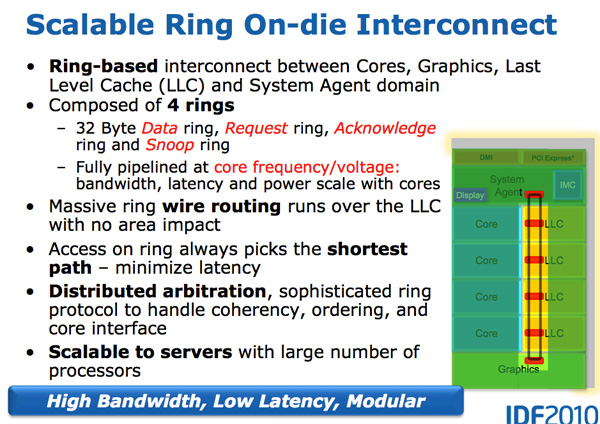
Architecturally, this is the same ring bus used in Nehalem EX and Westmere EX. Each core, each slice of L3 (LLC) cache, the on-die GPU, media engine and the system agent (fancy word for North Bridge) all have a stop on the ring bus.
The bus is made up of four independent rings: a data ring, request ring, acknowledge ring and snoop ring. Each stop for each ring can accept 32-bytes of data per clock. As you increase core count and cache size, your cache bandwidth increases accordingly.
Per core you get the same amount of L3 cache bandwidth as in high end Westmere parts - 96GB/s. Aggregate bandwidth is 4x that in a quad-core system since you get a ring stop per core (384GB/s).
L3 latency is significantly reduced from around 36 cycles in Westmere to 26 - 31 cycles in Sandy Bridge. We saw this in our Sandy Bridge preview and now have absolute numbers in hand. The variable cache latency has to do with what core is accessing what slice of cache.
Also unlike Westmere, the L3 cache now runs at the core clock speed - the concept of the un-core still exists but Intel calls it the “system agent” instead and it no longer includes the L3 cache.
With the L3 cache running at the core clock you get the benefit of a much faster cache. The downside is the L3 underclocks itself in tandem with the processor cores. If the GPU needs the L3 while the CPUs are downclocked, the L3 cache won’t be running as fast as it could had it been independent.
The L3 cache is divided into slices, one associated with each core although each core can address the entire cache. Each slice gets its own stop and each slice has a full cache pipeline. In Westmere there was a single cache pipeline and queue that all cores forwarded requests to, in Sandy Bridge it’s distributed per cache slice.
The ring wire routing runs entirely over the L3 cache with no die area impact. This is particularly important as you effectively get more cache bandwidth without any increase in die area. It also allows Intel to scale the core count and cache size without incurring additional ring-related die area.
Each of the consumers/producers on the ring get their own stop. The ring always takes the shortest path. Bus arbitration is distributed on the ring, each stop knows if there’s an empty slot on the ring one clock before.
The System Agent
For some reason Intel stopped using the term un-core, instead in Sandy Bridge it’s called the System Agent.
The System Agent houses the traditional North Bridge. You get a 16 PCIe 2.0 lanes that can be split into two x8s. There’s a redesigned dual-channel DDR3 memory controller that finally restores memory latency to around Lynnfield levels (Clarkdale moved the memory controller off the CPU die and onto the GPU).
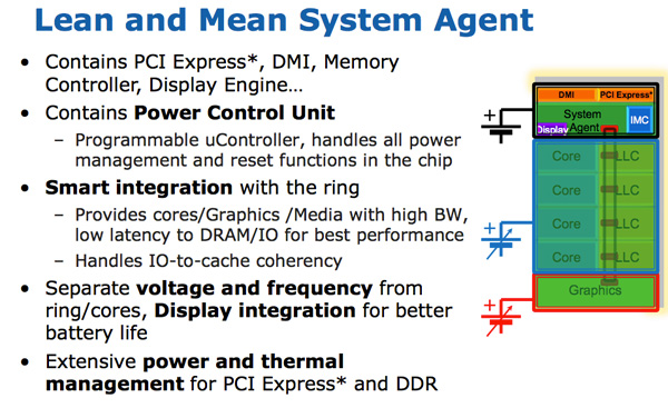
The SA also has the DMI interface, display engine and the PCU (Power Control Unit). The SA clock speed is lower than the rest of the core and it is on its own power plane.


62 Comments
View All Comments
name99 - Tuesday, September 14, 2010 - link
This is no secret. This is exactly Intel's tick-tock strategy that has been in place for years now.The one thing you have to keep in mind is that designing these CPUs now takes of order SEVEN YEARS (!!!) from conception to ship, which means that slips and mistakes do occur. Intel (and I guess AMD) have to make their best guess as to what the market will look like in seven years and sometimes they do guess incorrectly. Of course there is scope for small changes along the way closer to the release date, but not for changes in the grand strategy.
medi01 - Tuesday, September 14, 2010 - link
Agreed, it was two things: greed and the fact that AMD is currently not in a position to be a threat.tatertot - Tuesday, September 14, 2010 - link
"The value segments won’t see Sandy Bridge until 2012."You later show a roadmap slide which indicates Sandy Bridge in the value segment in Q3 2011.
Perhaps you meant "H2 '11" instead of "2012" ?
J_Tarasovic - Thursday, September 16, 2010 - link
I think that the roadmap probably refers to OEM shipments, whereas, Anand was probably referring to when consumers would actually be able to buy devices.iwodo - Tuesday, September 14, 2010 - link
I just realize that my computer will no longer scream when i do WebCam Video Conferencing with Skype!. With the Encoder Engine and Decoder Engine, all i am doing it feeding USB 3.0 data and move them around........yuhong - Tuesday, September 14, 2010 - link
"Back in the Core Duo days that was 80-bits of data. When Intel implemented SSE, the burden grew to 128-bits. ""Core Duo" Huh?
NaN42 - Tuesday, September 14, 2010 - link
No, it seems to be right. Core Duo belongs to the Pentium M microarchitecture which implemented the SSE registers as two 64bit registers. So the largest registers were the x87-registers, but I'm not sure whether upon register renaming the registers were really copied.aka_Warlock - Tuesday, September 14, 2010 - link
New CPU from Intel... and guess what?!! New SOCKET!! Lol.Intel do know how to milk the stupid cow.
bernpi - Sunday, November 14, 2010 - link
For most people it makes perfect sense to get a new socket. Most people don't buy every new CPU from Intel or AMD because it would be a waste of money. My current CPU is a Core2Duo Quad processor with a 775 socket, i skipped the nehalem generation and will buy a SandyBridge early next year. So why should i keep my motherboard and the old 775 socket? Of course i will buy a new motherboard for the new processor. So i think for most people this is not a real issue.Sahrin - Tuesday, September 14, 2010 - link
There's a lot of "neato" stuff that does a lot to improve the user experience by making the chip use its design resources more intelligently (smarter turbo - that 'comcast turbo-boost' feature should really make a difference for end users); but in terms of actual throughput it looks like Intel left FP performance the same; and there certainly isn't any new integer hardware.K11, on the other hand, doubled integer ALU's (though the raw number of execution units is now the same as in a Nehalem core) and added a half-width (compared to Intel) FP unit.
First, I'd be interested to see if the whizz-bangies AMD was talking about for the K11 FPU a year ago make the execution time for 128-bit FP instructions comparable, better than, or still slower than Intel's FPU .
Second, I'd be quadruple interested to see what impact the way AMD is allocating the new integer hardware is going to have on performance. A monolithic Nehalem core is going to be able to handle more complex (wider) threads better than a K11 core (that's a 2-integer and 1-FPU Bulldozer); but in SMT-mode (or pseudo-SMT mode) what happens? We know Intel experiences a performance hit in HTT mode which they are only able to offset because Nehalem is so wide. AMD thinks it isn't going to get the expected hit in the front end, and they won't have the thread-switching penalty that Intel does. My prediction is that 8-core K11/Bullzoder will crush Sandy Bridge in multithreaded FP-light workloads and be 5-20% slower in everything else (the possible exception being 128-bit floats).
I'm actually kind of disappointed by this update to Nehalem...Intel did a lot of "uncore" stuff and implemenated AVX. Where's our wider back-end? More execution hardware drives better single-thread performance...the rest is just undoing the damage from the CISC-RISC transition in the front end and OoO .