Intel's Sandy Bridge Architecture Exposed
by Anand Lal Shimpi on September 14, 2010 4:10 AM EST- Posted in
- CPUs
- Intel
- Sandy Bridge
The Ring Bus
With Nehalem/Westmere all cores, whether dual, quad or six of them, had their own private path to the last level (L3) cache. That’s roughly 1000 wires per core. The problem with this approach is that it doesn’t work well as you scale up in things that need access to the L3 cache.
Sandy Bridge adds a GPU and video transcoding engine on-die that share the L3 cache. Rather than laying out another 2000 wires to the L3 cache Intel introduced a ring bus.
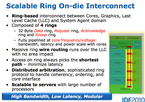
Architecturally, this is the same ring bus used in Nehalem EX and Westmere EX. Each core, each slice of L3 (LLC) cache, the on-die GPU, media engine and the system agent (fancy word for North Bridge) all have a stop on the ring bus.
The bus is made up of four independent rings: a data ring, request ring, acknowledge ring and snoop ring. Each stop for each ring can accept 32-bytes of data per clock. As you increase core count and cache size, your cache bandwidth increases accordingly.
Per core you get the same amount of L3 cache bandwidth as in high end Westmere parts - 96GB/s. Aggregate bandwidth is 4x that in a quad-core system since you get a ring stop per core (384GB/s).
L3 latency is significantly reduced from around 36 cycles in Westmere to 26 - 31 cycles in Sandy Bridge. We saw this in our Sandy Bridge preview and now have absolute numbers in hand. The variable cache latency has to do with what core is accessing what slice of cache.
Also unlike Westmere, the L3 cache now runs at the core clock speed - the concept of the un-core still exists but Intel calls it the “system agent” instead and it no longer includes the L3 cache.
With the L3 cache running at the core clock you get the benefit of a much faster cache. The downside is the L3 underclocks itself in tandem with the processor cores. If the GPU needs the L3 while the CPUs are downclocked, the L3 cache won’t be running as fast as it could had it been independent.
The L3 cache is divided into slices, one associated with each core although each core can address the entire cache. Each slice gets its own stop and each slice has a full cache pipeline. In Westmere there was a single cache pipeline and queue that all cores forwarded requests to, in Sandy Bridge it’s distributed per cache slice.
The ring wire routing runs entirely over the L3 cache with no die area impact. This is particularly important as you effectively get more cache bandwidth without any increase in die area. It also allows Intel to scale the core count and cache size without incurring additional ring-related die area.
Each of the consumers/producers on the ring get their own stop. The ring always takes the shortest path. Bus arbitration is distributed on the ring, each stop knows if there’s an empty slot on the ring one clock before.
The System Agent
For some reason Intel stopped using the term un-core, instead in Sandy Bridge it’s called the System Agent.
The System Agent houses the traditional North Bridge. You get a 16 PCIe 2.0 lanes that can be split into two x8s. There’s a redesigned dual-channel DDR3 memory controller that finally restores memory latency to around Lynnfield levels (Clarkdale moved the memory controller off the CPU die and onto the GPU).
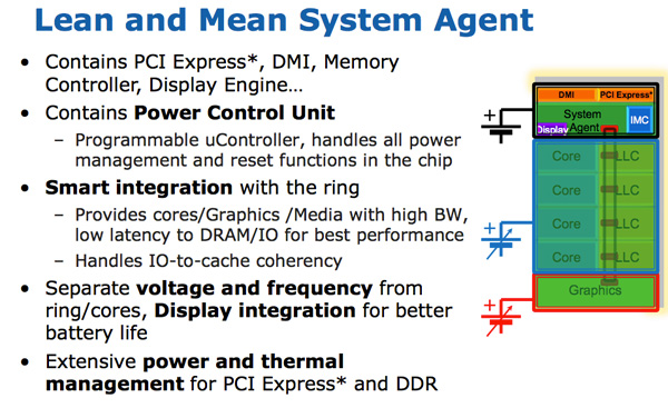
The SA also has the DMI interface, display engine and the PCU (Power Control Unit). The SA clock speed is lower than the rest of the core and it is on its own power plane.


62 Comments
View All Comments
FXi - Tuesday, September 14, 2010 - link
Only thing I am saddened by is that hybrid graphics apparently won't be "working" on the mobile high end chipset with the dual pci-e x8 lanes. It's extremely nice to have 2x a good modern mobile GPU, but still be able to switch to the Intel built in GPU when you want longer battery life on the road.That ability, in the 2920 was something I was truly hoping for.
The rest of its abilities are quite nice and very welcome. USB 3 really is something to be sure they didn't miss. But otherwise kudos Intel.
Drazick - Tuesday, September 14, 2010 - link
Anand, few questions with your permission:I wonder If we could use a Discrete Graphics Card and enable the Media Engine.
What about the DMI bus, Hasn't it become a bottleneck with SSD Drives and USB3?
Does Intel have planes to address it?
Thanks.
EricZBA - Tuesday, September 14, 2010 - link
Someone please release a decent 13.3 inch laptop using Sandy Bridge please.bitcrazed - Tuesday, September 14, 2010 - link
I have a sneaking suspicion that Intel will be at the core of Apple's next laptop platform refresh with both SandyBridge and LightPeak.Apple's MacBook lineup is starting to feel a little pressure from the other PC laptop vendors who are starting to produce some nicely designed tin and will need to stay current in order to continue to sell their products at such high premiums.
I'm imagining the next MacBook Pro lineup to offer 13" MBP's running i3 2120's and the 15" and 17" models running i5 2400/2500's or i7 2600's.
Apple already have their own dynamic integrated/discrete GPU switching technology (as do nVidia) and can make even better use of SB's integrated GPU augmented by a modest discrete GPU to deliver the performance that most users need but with much reduced power drain.
So how to differentiate themselves? LightPeak. Apple was the instigator of LightPeak to start with and Intel claimed at CES 2010 that it'd appear around a year later. That's next spring.
One thing's for sure: 2011 is going to be a VERY interesting year for new laptop and desktop devices :)
name99 - Tuesday, September 14, 2010 - link
LightPeak WITHOUT USB3 will go over like a lead zeppelin.There are already plenty of USB3 peripherals available. I have never in my life seen a LightPeak peripheral, or even a review or sneak peek of one. Light Peak is coming, but I'm not sure that 2011 is its year.
The rate at which CPU speeds now increases is low enough that very few buyers feel any sort of pressure to upgrade the machine they bough 3 years ago. Apple can't deal with that by simply offering new iMacs and MacBooks with the newest Intel offering, since no normal person is much excited by another 10% CPU boost.
They have done an adequate job of dealing with this so far by boosting battery life, something (some) portable users do care about.
They have done a mixed job of making more cores, hyperthreading and better GPUs a reason to upgrade. We have some low-level infrastructure in Snow Leopard, but we have fsckall user level apps that take advantage of this. Where is the multi-threaded Safari? Where is the iTunes that utilizes multiple cores, and the GPU for transcoding audio? Does FileVault use AES-NI --- apparently not.
But Apple has done an truly astonishingly lousy job of tracking the one remaining piece of obvious slowness --- IO. Still no TRIM, still no eSATA, still no USB3.
My point is that I don't know the Apple politics, but I do know that they are doing a very very bad job of shipping machines that compel one to upgrade. There is no need for me to upgrade my 3+yr old Penryn iMac, for example --- I'd get a replacement with more cores (not used by any of my software), a better GPU (but what I have plays video just fine), and most importantly, NO FASTER IO.
Adding LightPeak to this mix without USB3 is not going to help any. People are still going to hold off on upgrades until USB3 is available, and no-one is going to rush to buy a LightPeak system so that they can then NOT run any of the many unavailable LightPeak peripherals on the shelves at Fry's.
NaN42 - Tuesday, September 14, 2010 - link
On page 3: "Compared to an 8-core Bulldozer a 4-core Sandy Bridge has twice the 256-bit AVX throughput."WTF? 8*128 = 4*256. Based on the premise that the fp-scheduler of one Bulldozer module (two cores) can schedule e.g. one add and one mul avx-instruction per clock cycle, they have the same throughput. I think both architectures will have a delay for e.g. shuffling ymm-registers (compared to current xmm-instructions) because data has to be exchanged between different pipelines/ports (Hopefully the picture provided by Intel is correct). Perhaps the delay is smaller in Sandy Bridge cores. I expect some delays when one mixes floating-point and integer instructions on Sandy Bridge. (Currently I don't know, whether there exists a VEX prefix for xmm integer instructions. If there's no VEX prefix the delays will be great on both platforms.)
gvaley - Tuesday, September 14, 2010 - link
"...you get two 256-bit AVX operations per clock.""AMD sees AVX support in a different light than Intel. Bulldozer features two 128-bit SSE paths that can be combined for 256-bit AVX operations. "
So it's actually 8*256 = 4*2*256. At least this is how I see it.
NaN42 - Tuesday, September 14, 2010 - link
"So it's actually 8*256 = 4*2*256. At least this is how I see it. "Ok, my calculation was a bit different. 4*2*256 will be true, but only if you mix additions and multiplications. Whether AMD is 8*2*128 depends on the fp-scheduler (based on the premise that one SIMD unit consists of a fmul, fadd and fmisc unit or something similar)
NaN42 - Tuesday, September 14, 2010 - link
... one can do another floating point operation which goes through port 5, but the peak performance of additions and multiplications is more relevant in applications.Spacksack - Tuesday, September 14, 2010 - link
I think you are right. I would think bulldozer can manage the same theoreticakl throughput by issuing one combined FMA instruction (16 flop) / clock and module.More importantly Bulldozer will achieve hight throughput for all the existing SSE code by having two independent FMA units. I have no idea how Anand could make such a mistake.