Intel's 50Gbps Silicon Photonics Link: The Future of Interfaces
by Brian Klug on July 30, 2010 6:49 AM EST- Posted in
- Trade Shows
- Intel
- Photonics
- Laser
On Tuesday, Intel demonstrated the world’s first practical data connection using silicon photonics - a 50 gigabit per second optical data connection built around an electrically pumped hybrid silicon laser. They achieved the 50 gigabit/s data rate by multiplexing 4 12.5 gigabit/s wavelengths into one fiber - wavelength division multiplexing. Intel dubbed its demo the “50G Silicon Photonics Link.”
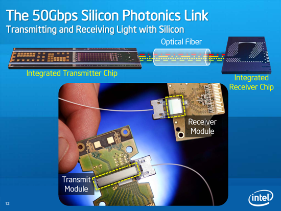
Fiber optic data transmission isn’t anything new - it’s the core of what makes the internet as we know it today possible. What makes Intel’s demonstration unique is that they’ve fabricated the laser primarily out of a low-cost, mass-produceable, highly understood material - silicon.
For years, chip designers and optical scientists alike have dreamt about the possibilities of merging traditional microelectronics and photonics. Superficially, one would expect it to be easy - after all, both fundamentally deal with electromagnetic waves, just at different frequencies (MHz and GHz for microelectronics, THz for optics).
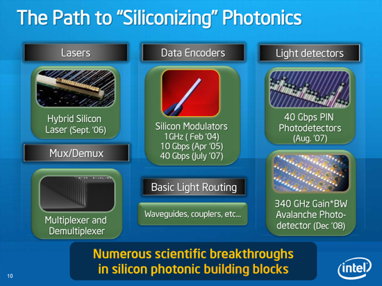
On one side, microelectronics deals with integrated circuits and components such as transistors, copper wires, and the massively understood and employed CMOS manufacturing process. It’s the backbone of microprocessors, and at the core of conventional computing today. Conversely, photonics employs - true to its name - photons, the basic unit of light. Silicon photonics is the use of optical systems that use silicon as the primary optical medium, instead of other more expensive optical materials. Eventually, photonics has the potential to supplant microelectronics with optical analogues of traditional electrical components - but that’s decades away.
Until recently, successfully integrating the two was a complex balance of manufacturing and leveraging photonics only when it was feasible. Material constraints have made photonics effective primarily as a long haul means of getting data from point to point. To a larger extent, this has made sense because copper traces on motherboards have been fast enough, but we’re getting closer and closer to the limit.


42 Comments
View All Comments
toktok - Sunday, August 1, 2010 - link
Pick 'n' mix motherboards!joshv - Monday, August 2, 2010 - link
Wonder if different parts of a chip couldn't use optical interconnects to talk to other parts of the chip, basically in free space above the chip. Basically just point the detectors and emitters at each other. The nice thing is that the optical paths can intersect each other with no penalty. Electrical paths have to be routed around each other in the various layers of the chip.Shadowmaster625 - Monday, August 2, 2010 - link
Doesnt this make it possible to place 8GB of DDR3 onto a single chip? Just stack a bunch of dies and wire them all to a silicon photonic transmitter, then connect that directly to the cpu. Also, shouldnt this make it possible to stack all the NAND flash you'd ever need onto one die? And then SSDs can be made with one memory chip. Replace SATA with silicon photonics, and it should be possible to have a 100GB/sec SSD. In other words, there would be no need for RAM at all...GullLars - Wednesday, August 4, 2010 - link
There's a couple of fundamental problems with your last part.First is the method of read/write and R/W asymmetry of NAND.
Second is latency. NAND is roughly 1000 times slower than DRAM.
It would be great for scaling bandwidth though, but then you have the problem of data parallelism and transfer sizes...
You would also need processing power for NAND upkeep (wear leveling, ECC, block management, channel management, etc), which would be a lot at 100GB/s.
Today, the fastest NAND dies are around 100MB/s(+?) for reads, so you would need to manage 10.000 dies (which wouldn't fit one package BTW XD) for 100GB/s.
EddyKilowatt - Monday, August 2, 2010 - link
... whatever you do, don't dumb down AnandTech! This was perfect for a lot of geeky folks out here. Who else puts things like "Laser = gain medium + resonator + pump" in one non-stuffy, easily understood, non-patronizing paragraph?A few decades ago when I was a cub engineer, my mentor predicted almost exactly this as the logical evolution of inter-chip links. I hope he's still around to see this finally hit the market.
How is Intel going to handle the I/O's to these optically-enabled chips? It's the only box on the "Siliconizing" viewgraph without a picture! Fiber is cheap but fiber termination is ex-pen-sive...
Cogman - Tuesday, August 3, 2010 - link
Optics have far more benefits over just "really high speed" For starters, optical cables can be VERY close together without causing any sort of interference. This is a big plus for people like motherboard designers. Now, they could stick ram anywhere on the board (not just right next to the CPU) They can overlap connectors, do whatever. It makes a big difference.Besides basically having no crosstalk / interference problems, Optical transmission has the added benefit of being able to send multiple signals down the same line (we probably aren't to the point of being able to realize that.) It is entirely possible that we could get to the point of having two optics lines running from the ram, one for upstream, the other for down. Each having the benefit of being able to send full 256/512 (or higher) bits of information in a single transmission cycle. We send data serially now because of interference problems, with optics, that would no longer be an issue, parallel data transmission would easily be able to overtake its serial counterpart.
Though, all the ultrahigh speed data transmission in the world doesn't mean a thing if the processor can't crunch the numbers fast enough.
has407 - Wednesday, August 4, 2010 - link
> Now, they could stick ram anywhere on the board (not just right next to the CPU) They can overlap connectors, do whatever.There's still speed-of-light constraints. For the foreseeable future, the closer, the better (that's the primary reason for the CRAY-1 physical structure--to reduce interconnect distance, not because it looked cool).
> Optical transmission has the added benefit of being able to send multiple signals down the same line (we probably aren't to the point of being able to realize that.)
We've been there and done that for years. It's called WDM or DWDM. Virtually all fiber-based communication today multiplexes multiple optical wavelengths/signals across a single fiber. That's how we get much more bandwidth without having to lay new fiber.
> We send data serially now because of interference problems, with optics, that would no longer be an issue, parallel data transmission would easily be able to overtake its serial counterpart.
Ummm...no. Parallel interconnects, regardless of medium, suffer from skew and the need for deskew. That always has, and always will be, a problem for parallel; optical interconnects do not fundamentally change the equation (although they minimize some problems). Thus the desire to reduce the number of parallel interconnects by using a smaller number of faster serial interconnects. Optics offers the option of significantly increasing serial interconnect speed, thus reducing the need for parallel interconnects and their associated problems.
I.e., the number of bits/sec that can be transferred over a single "wire" (or in this case fiber), minimizes the need for parallel interconnects. Maybe a few niche apps will need the augmented bandwidth that parallel can provide, but I have my doubts... Will WDM/DWDM scale fast enough? I bet it will scale faster/cheaper than parallel interconnects, at least for 99% of the market.
jpbattaille - Thursday, August 5, 2010 - link
Totally agree with this comment - the article seems to make abstraction of these facts.Optical speed of light in fiber is 200 m/s, in vacuum 300 m/s.
jpbattaille - Thursday, August 5, 2010 - link
Sorry, 20 cm /ns and 30 cm/nsPlugAndTweak - Wednesday, August 4, 2010 - link
This sounds very cool and promising on the paper.But what does it really mean to us as single end users?
This isn't the components themselves we are talking about that will get silicon photonics, that was WAY ahead in the future.
It's the interconnects.
I bet that even if we would get all the interconnects in the mobo;s with Silicon Photonics we wouldn't notice any dramatic differences even in very intensive stuff like Videoediting, 3d-rendering, software synthesizers and plug-ins in DAW;s and so on.
And would SSD;s REALLY be faster than any comparable technology today?
Even theoretically?
And take a look at tests where different memory speeds are done, there has always been minimal differences (often just 1-2 percent in average) when doing these tests. Increasing the bandwitdth in the interconnects won't have any dramatic difference in that aspect.
Not for us single power users.
For the big players with setups of loads of CPU;s and other components I could see the speed advantage.
And there are the other mentioned advantages for the single power user, like less power consumed, possibly smaller motherboards (if they find inexpensive cooling solutions).
Then there are all the advantages for the manufacturers with less interference and all the other stuff mentioned.
I really think that the ones that will benefit most from this is the manufacturers of the motherboard, much more than us single users.
Not until they get to the point of using it on the component level.