GlobalFoundries Plans to Expand Dresden and NY Fabs in Anticipation of 28/22nm
by Anand Lal Shimpi on May 31, 2010 11:44 PM EST- Posted in
- Trade Shows
- CPUs
- GlobalFoundries
Only a year has passed since AMD officially spun off its manufacturing division with the help of ATIC. The resulting GlobalFoundries have been busy getting its ducks in a row in preparation for inevitable battle with TSMC. It started with construction of Fab 8 (formerly GF Fab 2) in Saratoga County, NY due for revenue production in 2012. Today GF is announcing plans to expand Fab 8 before its completion and an expansion to Fab 1 (formerly AMD Fab 30/36) in Dresden.
Global also announced initial plans to create a similar cluster of fabs in Abu Dhabi. These clusters are placed on a site that can house three manufacturing modules, similar to what’s being expanded at Dresden and being built in Saratoga County. Given that GlobalFoundries’ majority shareholder is ATIC, an investment arm of the government of Abu Dhabi, the next location for fab expansion makes perfect sense.

At the end of last year, ATIC announced that it would acquire Chartered Semiconductor for $3.9 billion. The acquisition gave GlobalFoundries a 300mm fab in Singapore. The move wasn’t about taking out a competitor, but rather acquiring a customer base on aging manufacturing processes and giving them the option of migrating to smaller transistor geometries, something Chartered didn’t have the roadmap to do. A very smart move on GlobalFoundries’ part. To make room for the planned growth we have the aforementioned expansions at Fab 1 and Fab 8.
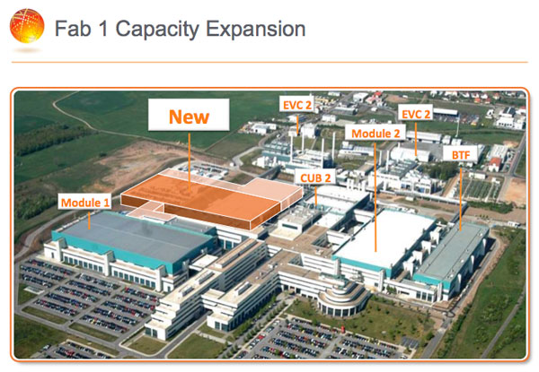
Fab 1 will get a new facility that can manufacture 45/40/28nm wafers and take Dresden’s total maximum output from 50,000 wafers per month to 80,000. The first production from this expansion will ship in 2011. We can also expect to see initial 22nm development done here, with Fab 1 eventually shifting to 22nm production over time.
Fab 8’s clean room will grow another 40% by the time it’s done. The original plans for Fab 8 targeted 35,000 wafer starts per month, but with the expansion we’re looking at a maximum of 60,000 with additional equipment.
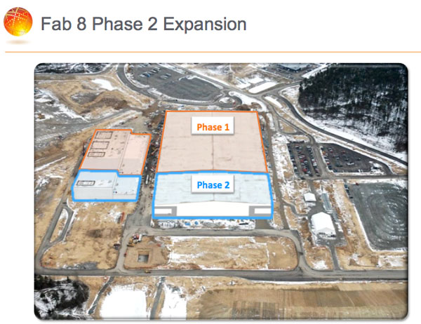
It’s not all good news though. Fab 8 is still expected to ship revenue generating wafers starting in 2012, but volume production won’t happen until 2013. Thankfully ATIC has very deep pockets.
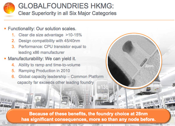
GlobalFoundries has often mentioned to me that if it had a customer willing to pay for it, it could offer transistor size and performance on par with Intel. In the past, AMD simply hadn’t been willing (or able) to pay for it. The 3rd bullet point on the slide below seems to make that same statement publicly.
A good AMD design coupled with a good process from GF could do some damage. Will Bulldozer be that design? It’s far too early to tell. Personally I’m more interested in seeing what a GPU manufactured at GlobalFoundries would look like.


11 Comments
View All Comments
Penti - Sunday, June 13, 2010 - link
Please there is no 30cm transistors. No 300nm for digital integrated circuits since a decade. Certainly not at a 300mm plant.Chartereds Fab was already on AMD APM process an collaborated with AMD and IBM (among others) and already produced AMD cpus since a few years back, which is why they have been bought.
CSM's fab had no such humongous process get over yourself, was certainly not locked to any particular node size, as I indicate they did manufacture down to 45nm. Many of AMDs 65nm processors is from there. They also produced at higher processes as they also had older 200mm plants. Also probably manufacturing semiconductors for other needs.
By doing that they also gained Chartereds other clients as customers, among like companies such as Broadcom and Qualcomm. Which also will be interested in capacity at Dresden or NY. Or at a upgraded Singapore plant.
My point though, AMD already utilized the 300mm fab in Singapore for processor manufacturing and GF wants to become a multivendor foundry. As they where experiencing problems it only came naturally. Also Asia is where most of the foundries are located any way. They will certainly upgrade the Singapore plant, they need the capacity it isn't about buying a customer stock. The 200mm fabs even have life in them as they do a lot of CMOS and RF and mixed signal ICs. The 300mm fab has a capacity of 50 000 wafers and that plant has been rated down to 40nm. It's a plant that handles SOI and technically is about equivalent to IBMs own plant. Of course allowing the tools to be compatible with plants also in Germany and NY it means the chips can be fabbed there to, but they desperately need that 50 000 wafers capacity in order to handle those existing customers. The fab was already at AMD/GFs APM process, it's not 32/28nm compatible as is though, but neither is any other plant.