Intel Unveils Moorestown and the Atom Z600, The Fastest Smartphone Platform?
by Anand Lal Shimpi on May 4, 2010 11:54 PM EST- Posted in
- Smartphones
- Intel
- Atom
- Mobile
- SoCs
When I wrote my first article on Intel's Atom architecture I called it The Journey Begins. I did so because while Atom has made a nice home in netbooks over the years, it was Intel's smartphone aspirations that would make or break the product. And the version of Atom that was suitable for smartphone use was two years away.
Time sure does fly. Today Intel is finally unveiling its first Atom processors for smartphones and tablets. Welcome to Moorestown.
Craig & Paul’s Excellent Adventure
Six years ago Intel’s management canned a project called Tejas. It was destined to be another multi-GHz screamer, but concerns over power consumption kept it from coming to fruition. Intel instead focused on its new Core architecture that eventually led to the CPUs we know and love today (Nehalem, Lynnfield, Arrandale, Gulftown, etc...).
When a project gets cancelled, it wreaks havoc on the design team. They live and breathe that architecture for years of their lives. To not see it through to fruition is depressing. But Intel’s teams are usually resilient, as is evidenced by another team that worked on a canceled T-project.
The Tejas team in, er, Texas was quickly tasked with coming up with the exact opposite of the chip they had just worked on: an extremely low power core for use in some sort of a mobile device (it actually started as a low power core as a part of a many core x86 CPU, but the many core project got moved elsewhere before the end of 2004). A small group of engineers were first asked to find out whether or not Intel could reuse any existing architectures in the design of this ultra low power mobile CPU. The answer quickly came back as a no and work began on what was known as the Bonnell core.
No one knew what the Bonnell core would be used in, just that it was going to be portable. Remember this was 2004 and back then the smartphone revolution was far from taking over. Intel’s management felt that people were either going to carry around some sort of mobile internet device or an evolution of the smartphone. Given the somewhat conflicting design goals of those two devices, the design team in Austin had to focus on only one for the first implementation of the Bonnell core.
In 2005, Intel directed the team to go after mobile internet devices first. The smartphone version would follow. Many would argue that it was the wrong choice, after all, when was the last time you bought a MID? Hindsight is 20/20 and back then the future wasn’t so clear. Not to mention that shooting for a mobile extension of the PC was a far safer bet for a PC microprocessor company than going after the smartphone space. Add in the fact that Intel already had a smartphone application processor division (XScale) at the time and going the MID route made a lot of sense.
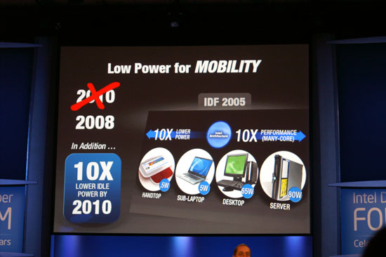
The team had to make an ultra low power chip for use in handheld PCs by 2008. The power target? Roughly 0.5W.
Climbing Bonnell
An existing design wouldn’t suffice, so the Austin team lead by Belli Kuttanna (former Sun and Motorola chip designer) started with the most basic of architectures: a single-issue, in-order core. The team iterated from there, increasing performance and power consumption until their internal targets were met.
In order architectures, as you may remember, have to execute instructions in the order they’re decoded. This works fine for low latency math operations but instructions that need data from memory will stall the pipeline and severely reduce performance. It’s like not being able to drive around a stopped car. Out of order architectures let you schedule around memory dependent operations so you can mask some of the latency to memory and generally improve performance. Despite what order you execute instructions, they all must complete in the program’s intended order. Dealing with this complexity costs additional die area and power. It’s worth it in the long run as we’ve seen. All Intel CPUs since the Pentium Pro have been wide (3 - 4 issue), out of order cores, but they also have had much higher power budgets.
As I mentioned in my original Atom article in 2008 Intel was committed to using in order cores for this family for the next 5 years. It’s safe to assume that at some point, when transistor geometries get small enough, we’ll see Intel revisit this fundamental architectural decision. In fact, ARM has already gone out of order with its Cortex A9 CPU.
The Bonnell design was the first to implement Intel’s 2 for 1 rule. Any feature included in the core had to increase performance by 2% for every 1% increase in power consumption. That design philosophy has since been embraced by the entire company. Nehalem was the first to implement the 2 for 1 rule on the desktop.
What emerged was a dual issue, in-order architecture. The first of its kind from Intel since the original Pentium microprocessor. Intel has learned a great deal since 1993, so reinventing the Pentium came with some obvious enhancements.
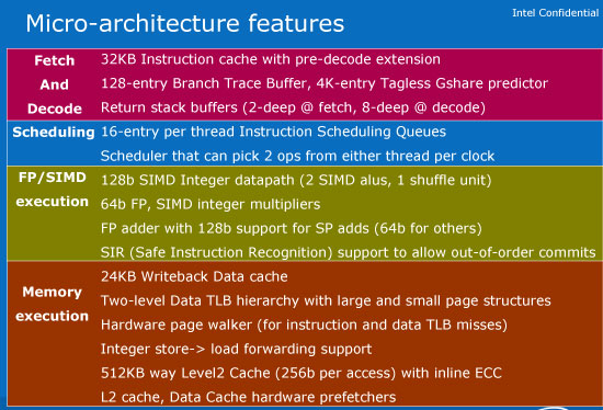
The easiest was SMT, or as most know it: Hyper Threading. Five years ago we were still arguing about the merits of single vs. dual core processors, today virtually all workloads are at least somewhat multithreaded. SMT vastly improves efficiency if you have multithreaded code, so Hyper Threading was a definite shoe in.
Other enhancements include Safe Instruction Recognition (SIR) and macro-op execution. SIR allows conditional out of order execution depending if the right group of instructions appear. Macro-op execution, on the other hand, fuses x86 instructions that perform related ops (e.g. load-op-store, load-op-execute) so they go down the pipeline together rather than independently. This increases the effective width of the machine and improves performance (as well as power efficiency).
Features like hardware prefetchers are present in Bonnell but absent from the original Pentium. And the caches are highly power optimized.
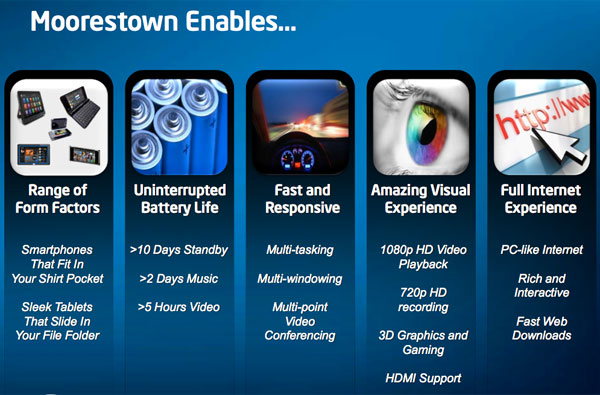
Bonnell refers to the core itself, but when paired with an L2 cache and FSB interface it became Silverthorne - the CPU in the original Atom. For more detail on the Atom architecture be sure to look at my original article.


67 Comments
View All Comments
strikeback03 - Thursday, May 6, 2010 - link
Actually, at least on Verizon, there are not many phones that last more than 2-3 days with relatively light use (5-10 min talk, 20-30 txt per day). This is actually something that has gone down in the past few years, as even basic phones get flashier UIs and use more power to run them. And while I support having some phones with weeklong standby time, I am fine with charging my phone or switching batteries every night so long as the phone can last a day in moderate use, which the Snapdragon phones typically can. I like to be able to access more than talk and text on the go.v12v12 - Monday, May 10, 2010 - link
WOW... standing ovation... All of my Droid friends are laughable! Constantly tethered to a power outlet! Always doing something useless and for sure entertainment Vs thinking quietly with their minds... pretty soon "dude I gotta go, my phone is about to die," yeah umm just how many hours have your spent actually TALKING on the dang thing vs playing around with it constantly like some personalized TOY?Battery life should be much more focused upon... The cattle-minded consumers are at it again; now tell me, had to only have 1 car, would you also buy a car that gets the WORST miles per gallon, but has a bunch of silly go-fast features that have you constantly at the fuel pump Vs getting to where you need/should be? Course that's why people usually own 2 cars to separate those needs Vs desires.... Today's "Ferrari" phones have the everyday idiot rambling along, bumping into shit, with their heads constantly fixated on the "screen," like drones. Talking...(?) haha you rarely see people talking with these things, it's just constant "entertainment," even in the most hindering places and social situations. So everyone's got a "Ferrari" phone, but end up trying to use it like a honda; sorry it just doesn't work like that. Faster = more fuel, LESS actual usefulness.
__I'd rather have a phone with a decent amount of enjoyable features, that I can actually take with me on a trip to places that may or may not have power ON-DEMAND lol..
juampavalverde - Wednesday, May 5, 2010 - link
The article and the new product is really interesting, but intel aint ready yet for smartphones, actually this moorestown platform looks much more interesting for pads and handhelds, having more space for such amount of chips, also being x86 with a custom linux. something like an ipad powered by this kind of atom starts to make sense, both from the performance and the battery lifeWorldMage - Thursday, May 6, 2010 - link
The interesting thing about all of the power draw figures given is that they were for workloads wherethe ATOM would be doing almost nothing. Video decode is done by the video decode HW where the
atom might wake up every few seconds to load the next batch of data, similarly for audio playback and
talk time (as you point out cellular modem is the only thing doing work). The thing that gets closest is web browsing, but assuming they are browsing 'static' pages (i.e. no Flash) the atom does a bit of work and probably sits essentially idle for easily 90% of the time.
So it's not surprising they are in the same ballpark as other SOC's for those workloads since they seem to essentially be using the same HW blocks as the competing SOC's. I think it's very telling that all of the power consumption figures from Intel were for essentially non-Atom work loads.
To which you might say "so what?" if those are the work flows that you care about, but that would ignore the fact that the whole point of the atom is to enable "fancy" UI's (and perhaps games) with lots of animation and stuff happening in the background and actually making use of the power of an ATOM.
If you can't actually power the ATOM for an hour of actual use (browsing contacts, checking flights, web pages with Flash ads etc) won't the smart phone be almost worthless?
Th3Loonatic - Thursday, May 6, 2010 - link
On page 3 of the article you misnamed the chips. The one on the left is Lincroft and the one on the right is Langwell.Electrofreak - Friday, May 7, 2010 - link
Anand, Cortex A8 on the 65 nm feature size is reported to use about 0.59 mW per MHz under load, and Cortex A8 on the 45 nm feature size is reported to use 20-30% less than that. For a little bit of added beliveability, Qualcomm's Snapdragon sips in the vicinity of 0.5 mW per MHz on the 65 nm scale, though that may be under optimal circumstances / marketing spin.Ultimately it's roughly half the power consumption Moorestown is reporting. And we notice that nowhere does Intel actually compare their power consumption figures to ARM's.
Additionally, I was under the impression that the A4 had a dual-channel memory controller. I would guess LPDDR2 memory as well, but your guess is as good as mine.
I suspect the S5L8930 in the A4 is a PA Semi (remember Apple bought them) reworked Samsung S5PV210, the dual-channel controller tablet / MID-oriented sister chip to the Samsung Hummingbird S5PC110 (which uses a single-channel controller with LPDDR2 support, if my resources are to be trusted.)
pradeepcvk - Tuesday, November 1, 2011 - link
Anand liked your brief of S0Ix wrt Meego. I wonder how would it work with windows ACPI.could you please have an article for the same.