Gigabyte GA-P55-UD6 - The Big Kahuna
by Gary Key on July 16, 2009 12:28 PM EST- Posted in
- Gary's First Looks
The upcoming launch of the Intel P55 and associated S1156 based processors is starting to resemble the buildup we noticed before the P965/Core 2 launch. We are already swamped with weekly press releases touting specifications and feature information from all of the P55 launch partners. In fact, revisions are occurring on an almost daily basis as each manufacturer tweaks their final product designs in hopes of capturing your hard earned dollars.
While aesthetics, features, and colors are an integral part of the motherboard design, ultimately how well it performs is based on the quality of components and BIOS design. We also happen to rate warranty and customer support at the top of this list but eventually it always comes back to performance or price for most users.
When it comes to performance, Gigabyte is usually a name that always comes up in the course of a conversation when discussing motherboards. They typically have extremely solid products and occasionally will hit one of those grand slam home runs with a product like the GA-EP45-UD3P, a board that offers the right blend of features, performance, support, price, and character.
The reason we bring this up is that the GA-P55-UD6 is already invoking the same feelings for us. Well, all except price as this will be Gigabyte's premium P55 offering. However, this board offers a lot for the money and is certainly targeting the enthusiast. Obviously, we cannot discuss performance yet, but the i5 is going to surprise a lot people, especially those buying into the lower end i7 market.
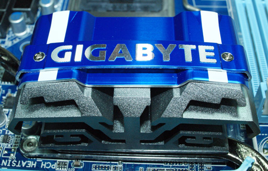
Even without the Gigabyte name plate on the P55 heatsink, taking one look at the layout and color scheme of this board instantly identifies its heritage. In fact, this design has not changed since we first looked at it during Computex this year. Gigabyte tossed the kitchen sink at this board and it stuck, but somehow it all works together without appearing to be too busy. We are not big fans of the floppy drive port and even IDE is starting to irritate us on the enthusiast boards, although one justification for IDE comes from the extreme overclocking community. In the quest to push PCIe speeds as far as possible the user can end up with some nasty SATA hard drive crashes that usually corrupt the operating system. So it turns out that an IDE drive can still be an overclockers best friend in certain situations.
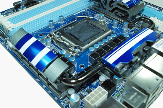
Hello 24-phase VRM technology. As with the space race and horsepower wars a few decades ago, we are now officially witnessing a Phase race in the motherboard industry. Does a greater number of phases actually improve clocking or temperatures, not necessarily, in fact, it can do just the opposite if designed poorly. The good news is that Gigabyte appears at first glance to have done their homework in this area. Exactly what the true advantages of this design compared to the 8-phase or 12-phase setups utilized by other companies is something we are testing at this moment.
Gigabyte continues on with their Ultra Durable 3 technology that consists of high quality solid capacitors, low RDS(on) MOSFETs, and ferrite core chokes plus their custom "Dynamic Energy Savings" technology that will throttle this board down to four-phases at idle or low load situations.
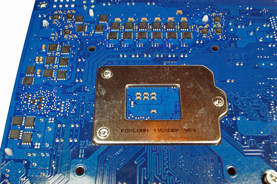
Due to the real estate involved in placing a 24-phase VRM setup on the board, the majority of MOSFETs and Intersil phase doublers are located on the back of the board. Considering some of the MOSFET temperatures we regularly see when overclocking the X58 motherboards, this area does cause us some concern for users who test on an open bench since airflow and heat dissipation under the board will be severely blocked.
Otherwise, the area is open and easily accommodated our larger air coolers and water blocks. On a side note, this will be an eight layer PCB design.
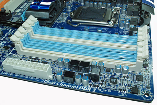
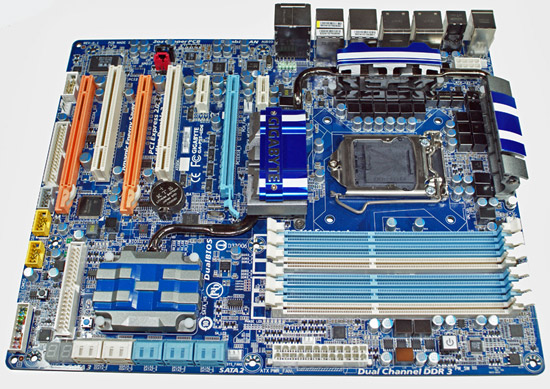
A first for the P55 platform is the inclusion of six memory slots instead of the standard four slot designs we are seeing on the other boards. Unlike the i7/X58 platform that supports and thrives on triple-channel memory performance, the P55/Lynnfield employs a dual-channel setup. We think the inclusion of the two additional memory slots is strictly for expansion possibilities. Gigabyte claims DDR3-2000+ memory capabilities and we fully expect to see those speeds when the board launches.
The 24-pin ATX power connector is located in a convenient location as is the power on/off switch. We do have to wonder why the clear CMOS, reset, and power switches are located at different points on the board.
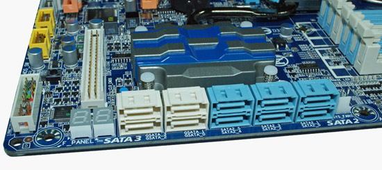
One of the more interesting areas on the board houses the various SATA ports (four 6Gb/s Marvell ports, six 3Gb/s P55 ports), LED debug display, clear CMOS and reset switches, and IDE drive port. Hiding underneath the heatsink is two Marvell 88SE9123 6Gb/s SATA chipsets that also provide IDE support. Contrary to reports on various forums and websites, it does appear the manufacturers are rethinking their recent decisions to drop the Marvell controller until the various hardware and driver problems are solved. It is too late in the process to qualify other controllers at this point for the majority of boards that were to include this chipset.
As such, it appears that Gigabyte (waiting on ASUS' official statement) is thinking they will leave the Marvell controller on the board and if 6G/s performance is not working properly, then the additional ports will be downgraded to 3Gb/s specifications. The "official" Marvell position is that the 88SE9123 controller suffers from PATA performance problems and that 6Gb/s SATA operation is not affected. However, after speaking with the motherboard suppliers and looking at our own test results, PATA performance/stability appears fine and 6Gb/s SATA performance is just not up to speed yet. Where the disconnect is between the motherboard engineers and Marvell is something we are trying to figure out at this point.
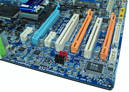
The P55-UD6 offers an abundance of expansion slots with an excellent layout. There are three PCIe x16 slots (x16/x4 or x8/x8/x4), two PCIe x1 slots, and two PCI slots. The Lynnfield processor series supports 16 PCIe 2.0 lanes and those lanes are assigned for graphics duty. The first x16 slot normally runs with 16 lanes and if you install a multi-GPU setup for CrossFire or SLI, then both slots run at x8. Truthfully, except for trying to set a benchmark record, the performance differences between dual x16 and dual x8 PCIe 2.0 is minimal at best in actual applications. The third x16 slot runs at x4 electrical and those lanes run off the P55 chipset.
Due to the performance hit of the DMI interface, NVIDIA has already informed the motherboard suppliers than they will not support SLI with this slot. We expect the same from AMD in regards to CrossFire X. We know of a few suppliers who have been toying with the NF200 bridge slot in order to run dual x16 or TriSLI on the P55 platform. So far, this concept has been problematic in the labs with performance and stability suffering to some degree at this stage in the game.
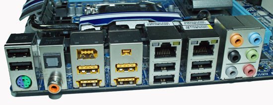
This I/O panel is loaded and ready for action. Gigabyte includes a combo PS/2 port, six USB 2.0 ports, two eSATA ports (JM362), two Gigabit Ethernet ports, IEEE 1394a port, optical and coaxial S/PDIF outputs, and the audio panel (Realtek ALC 889a). The Gigabit Ethernet controllers are courtesy of the Realtek RTL8111D chipset that features Smart Dual LAN technology. Simply put, if one controller fails, the board will automatically switch over to the other controller without the need to swap ports or run a second cable. Also, teaming is supported with a theoretical throughput of 2Gb/s, although actual throughput is far lower depending on your network setup.
That is it for now. Gigabyte is very interested in your thoughts on the design and feature list, so please feel free to leave comments.


54 Comments
View All Comments
crackedwiseman - Friday, July 17, 2009 - link
OK, 24-phase power seems a bit much... I'm all for enthusiast hardware (as a temporarily budget-constrained enthusiast myself) but there are other things you can use that PCB space for. What about digital PWMs? I don't have any numbers to quote, but having used them on DFI's UT X58 board, they seem to make a difference. Yes, they run hot, but with all the aluminum necessary for cooling a 24-phase solution, I'm sure that some copper could have been used for an 8 to 12 phase digital solution (the 10-phase PWM solution on EVGA's X58 classified is rated at 600 watts, and it would be difficult to cool even that much without cold-bugging the Intel silicon).Fewer phases leave room for other ICs, which brings me to my next point: why not use a PLX PCI express switch like the PEX 8647 or 8648 (or 8649 for the triple or quad GPU crowd)? The 8647 is (if I'm not mistaken) used on AMD's 4870x2 as part of the reference design, and its more versatile brother, the 8648 is capable of quad PCI-E x8 (among other configurations); the latency of these solutions is only 140ns, relatively small compared to the overall latency of PCI express. Larger solutions (admittedly, with 30ns more latency) could also connect to the troublesome Marvell SATA3 (6gb/s) chip, and could be used to disable it by simple disconnection until stable firmware shows itself. This is far better than dabbling with the hot and slow NF200 bridge from NVIDIA - the latency from that solution is noticeable in benchmarks, whereas the 4870x2's PLX solution is essentially equal in performance to 2 4870s in crossfire.
weevil - Friday, July 17, 2009 - link
Soon we'll have 48phase power!!! Is it really necessary or is just so they can say they have more phases than ASUS?Stele - Sunday, July 19, 2009 - link
[quote]As with the space race and horsepower wars a few decades ago, we are now officially witnessing a Phase race in the motherboard industry.[/quote]This race started way back c.2002, courtesy of Gigabyte no less, with their 6-phase power boards. IMHO there's a very real danger that it's all just about paper features and marketing gimmicks to entice the (very numerous) clueless average Joe. Since then the other brands have had to keep up with the Joneses in the game, including Asus which at that time was conservative but solid.
As you pointed out, one question is whether it's really necessary; a 6-8 phase PWM with sufficient decoupling capacitance and properly selected inductors would already bring the output ripple within the CPU's required specs. If the problem is maximum output current capability, then, IMHO it would be better to have a design using, say, 2x 140A pulse capable MOSFETs than 10x 28A pulse capable MOSFETs just to make it look impressive in the marketing brochures and photos. Or worse, it may be a case of 10x say, 20A to save cost yet still look cool (since nobody would think that a circuit with a larger number of parts could be inferior to one with less right? Right??).
As crackedwiseman noted, there're more efficient ways to use the PCB space, to say nothing of saving time, effort and cost in trying to route through so many components during PCB design. Unfortunately, things like circuit and board design quality - e.g. the difference between a circuit that has to handle up to 100A but is designed to handle 200, vs one that's designed to handle just 100 - are unquantifiable and not immediately apparent until sometime down the line - not the few weeks that reviewers get to play with it, which some manufacturers might try to count on.
One question at this point: is it really 24-phase or is it just a smaller number of phases with parallel driver/MOSFET trees? A good example was the Asus boards that used the ADP3198 PWM controller - claimed 8 phases but was more of 4 phases with each phase having 2 sets of driver/MOSFETs in place of the usual 1 to provide the "doubling".
Wwhat - Tuesday, July 21, 2009 - link
Isn't it the other way around? Wouldn't we have benefited from 24 phase long ago but only because of technological development it can now finally be done in an economical fashion?