Since NVIDIA did not send out review samples for the G(T) 200 series last year, we’ve been slowly building up our database of results as cards have arrived from the vendors themselves. We saw the GT 220 late last year, and last month we finally saw the GT 240. Thanks to MSI, today we’ll be looking at the final card in the (G)T 200 series: the GeForce 210. The specific card we’re looking at is MSI’s N210-MD512H.
| 9600GT | GT 220 | 9500GT |
9400GT
|
G 210 | |
| Stream Processors | 64 | 48 | 32 | 16 | 16 |
| Texture Address / Filtering | 32 / 32 | 16 / 16 | 16 / 16 | 8 / 8 | 8 / 8 |
| ROPs | 16 | 8 | 8 | 4 | 4 |
| Core Clock | 650MHz | 625MHz | 550MHz | 550MHz | 589MHz |
| Shader Clock | 1625MHz | 1360MHz | 1400MHz | 1400MHz | 1402MHz |
| Memory Clock | 900MHz (1800MHz effective) GDDR3 | 900MHz (1800MHz effective) GDDR3 | 400MHz (800MHz effective) DDR2 | 400MHz (800MHz effective) DDR2 | 500MHz (1000Mhz effective) DDR2 |
| Memory Bus Width | 256-bit | 128-bit | 128-bit | 128-bit | 64-bit |
| Frame Buffer | 512MB | 512MB | 512MB | 512MB | 512MB |
| Transistor Count | 505M | 486M | 314M | 314M | 260M |
| Manufacturing Process | TSMC 55nm | TSMC 40nm | TSMC 55nm | TSMC 55nm | TSMC 40nm |
| Price Point | $69-$85 | $69-$79 | $45-$60 | $40-60 | $30-$50 |
Like the GT 220, the G210 started life over the summer as an OEM-only card, earning its wings for a public launch in October along-side the GT 220. G210 is based on GT218, the smallest member of NVIDIA’s DirectX 10.1 GPU lineup, built out of 260M transistors and measuring a mere 57mm2 on TSMC’s 40nm process. As a product it replaces NVIDIA’s similar 9400GT, while in terms of pricing it replaces the slower 8400 GS.

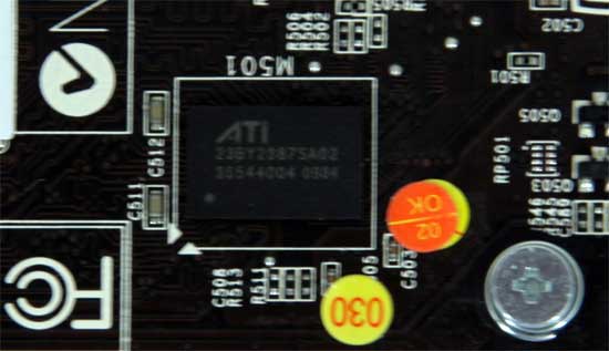
Coupled with the GT218 GPU on the G210 is 512MB of DDR2 RAM, using the customary 64bit memory bus. Interestingly, unlike most other entry-level products, the G210 only comes in 1 memory configuration: 512MB. Even more interesting are the DDR2 chips on our MSI card – 4 chips we can’t identify bearing the ATI logo.
Since the G210 is intended to replace the 9400GT, the GPU configuration is basically the same, composed of 16 SPs, 8 TMUs, and 4 ROPs. The clocks are 589MHz for the core, 1402MHz for the shaders, and 500MHz (1000MHz effective) for the RAM. Compared to the GT 220, this gives the G210 around 30% of the shader power, 50% the texture and ROP power, and 27% of the memory bandwidth. All of this consumes 30W under load, and less than 7W when idling.
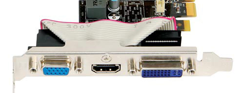
The G210 is a low-profile card, the only reference card to be that way out of NVIDIA’s entire 200-series lineup. NVIDIA’s reference design (not that anyone quite uses it) is a single-slot card with a similarly wide active cooler. For our MSI card, MSI has forgone that for a passive design, using a single double-wide heatsink. Most G210 cards do use some form of an active cooler, so MSI’s N210 is fairly unique in that regard.
Since the G210 is a low-profile card, the port configurations are as expected: 1 DVI, 1 HDMI or DisplayPort, and then the detachable VGA port. In the case of MSI's card, they have gone with an HDMI port as the second digital port, while the VGA port can be used on a full-profile bracket or a second bracket in a low-profile case.
Finally, in terms of pricing, the G210 is the ultimate budget card. With the MSI card going for only $30 after rebate, it’s for all practical purposes as cheap as a video card can get. Even the DDR2 version of the Radeon HD 5450 we reviewed last week goes for nearly 50% more. In terms of pricing this makes its competitors the GeForce 8400GS and the DDR2-based Radeon HD 4350, the latter of which is also its closest competitor to in terms of feature parity. It goes without saying that this is the ultimate entry-level card, and performs accordingly.


24 Comments
View All Comments
hwhacker - Tuesday, February 16, 2010 - link
Hmm, maybe he knows something we don't?Last I heard circulating AMD was going to get (sample?) product from both TSMC and GF on 32nm, but that got all borked when TSMC cancelled 32nm. As such, now they will transition to each company's respective 28nm process instead. This is said to have messed up Northern Islands' release, but may result in a better (not just smaller/faster) product. Who knows if that's true. All things being equal, I'm sure AMD would like to use 28nm bulk at GF.
As for nVIDIA, it's been interesting to watch. First they said absolutely not to GF, then 40nm at TSMC happened. After that Jensen was said to be in talks with GF, publically said some good things about GF over TSMC (likely because they're angry about 40nm RE: Fermi and used it for intimidation) and that's all we know. All things being equal, I'm sure nVIDIA would like to use 28nm bulk at TSMC.
Natfly - Tuesday, February 16, 2010 - link
You're right, both companies canned their 32nm bulk processes. So either the author is insinuating that nVidia is going to switch to 32nm SOI or he means 28nm.Ryan Smith - Tuesday, February 16, 2010 - link
He means 28nm.Natfly - Tuesday, February 16, 2010 - link
My apologies, I would have referred to you by name if I wasn't too lazy to go back to the article from the comments page to check :P