The RV870 Story: AMD Showing up to the Fight
by Anand Lal Shimpi on February 14, 2010 12:00 AM EST- Posted in
- GPUs
The Payoff: How RV740 Saved Cypress
For its first 40nm GPU, ATI chose the biggest die that made sense in its roadmap. That was the RV740 (Radeon HD 4770):
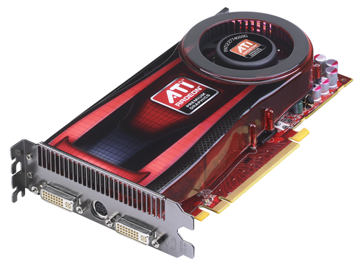
The first to 40nm - The ATI Radeon HD 4770, April 2009
NVIDIA however picked a smaller die. While the RV740 was a 137mm2 GPU, NVIDIA’s first 40nm parts were the G210 and GT220 which measured 57mm2 and 100mm2. The G210 and GT220 were OEM-only for the first months of their life, and I’m guessing the G210 made up a good percentage of those orders. Note that it wasn’t until the release of the GeForce GT 240 that NVIDIA made a 40nm die equal in size to the RV740. The GT 240 came out in November 2009, while the Radeon HD 4770 (RV740) debuted in April 2009 - 7 months earlier.
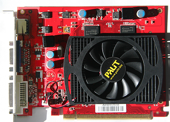
NVIDIA's first 40nm GPUs shipped in July 2009
When it came time for both ATI and NVIDIA to move their high performance GPUs to 40nm, ATI had more experience and exposure to the big die problems with TSMC’s process.
David Wang, ATI’s VP of Graphics Engineering at the time, had concerns about TSMC’s 40nm process that he voiced to Carrell early on in the RV740 design process. David was worried that the metal handling in the fabrication process might lead to via quality issues. Vias are tiny connections between the different metal layers on a chip, and the thinking was that the via failure rate at 40nm was high enough to impact the yield of the process. Even if the vias wouldn’t fail completely, the quality of the via would degrade the signal going through the via.
The second cause for concern with TSMC’s 40nm process was about variation in transistor dimensions. There are thousands of dimensions in semiconductor design that you have to worry about. And as with any sort of manufacturing, there’s variance in many if not all of those dimensions from chip to chip. David was particularly worried about manufacturing variation in transistor channel length. He was worried that the tolerances ATI were given might not be met.
![]()
A standard CMOS transistor. Its dimensions are usually known to fairly tight tolerances.
TSMC led ATI to believe that the variation in channel length was going to be relatively small. Carrell and crew were nervous, but there’s nothing that could be done.
The problem with vias was easy (but costly) to get around. David Wang decided to double up on vias with the RV740. At any point in the design where there was a via that connected two metal layers, the RV740 called for two. It made the chip bigger, but it’s better than having chips that wouldn’t work. The issue of channel length variation however, had no immediate solution - it was a worry of theirs, but perhaps an irrational fear.
TSMC went off to fab the initial RV740s. When the chips came back, they were running hotter than ATI expected them to run. They were also leaking more current than ATI expected.
Engineering went to work, tearing the chips apart, looking at them one by one. It didn’t take long to figure out that transistor channel length varied much more than the initial tolerance specs. If you get a certain degree of channel length variance some parts will run slower than expected, while others would leak tons of current.
Engineering eventually figured a way to fix most of the leakage problem through some changes to the RV740 design. The performance was still a problem and the RV740 was mostly lost as a product because of the length of time it took to fix all of this stuff. But it served a much larger role within ATI. It was the pipe cleaner product that paved the way for Cypress and the rest of the Evergreen line.
As for how all of this applies to NVIDIA, it’s impossible to say for sure. But the rumors all seem to support that NVIDIA simply didn’t have the 40nm experience that ATI did. Last December NVIDIA spoke out against TSMC and called for nearly zero via defects.
The rumors surrounding Fermi also point at the same problems ATI encountered with the RV740. Low yields, the chips run hotter than expected, and the clock speeds are lower than their original targets. Granted we haven’t seen any GF100s ship yet, so we don’t know any of it for sure.
When I asked why it was so late with Fermi/GF100, NVIDIA pointed to parts of the architecture - not manufacturing. Of course, I was talking to an architect at the time. If Fermi/GF100 was indeed NVIDIA’s learning experience for TSMC’s 40nm I’d expect that its successor would go much smoother.
It’s not that TSMC doesn’t know how to run a foundry, but perhaps the company made a bigger jump than it should have with the move to 40nm:
| Process | 150nm | 130nm | 110nm | 90nm | 80nm | 65nm | 55nm | 40nm |
| Linear Scaling | - | 0.866 | 0.846 | 0.818 | 0.888 | 0.812 | 0.846 | 0.727 |
You’ll remember that during the Cypress discussion, Carrell was convinced that TSMC’s 40nm process wouldn’t be as cheap as it was being positioned as. Yet very few others, whether at ATI or NVIDIA, seemed to believe the same. I asked Carrell why that was, why he was able to know what many others didn’t.
Carrell chalked it up to experience and recounted a bunch of stuff that I can’t publish here. Needless to say, he was more skeptical of TSMC’s ability to deliver what it was promising at 40nm. And it never hurts to have a pragmatic skeptic on board.


132 Comments
View All Comments
simtex - Sunday, February 21, 2010 - link
Excellent article ;) Insider info is always interesting, makes me a little more happy about my -50% AMD stocks, hopefully they will one go up again.NKnight - Wednesday, February 17, 2010 - link
Great read.- Friday, February 19, 2010 - link
you should write a (few)book(s); of course in multi eReader formats
asH
- Saturday, February 20, 2010 - link
Nvidia blames sales shortfall on TSMChttp://www.eetimes.com/news/latest/showArticle.jht...">http://www.eetimes.com/news/latest/show...E1GHPSKH...
one dot you didnt connect in the article was AMD's foundry experience, which gives AMD a big advantage over NVIDIA; must have been an oversight?
asH
truk007 - Tuesday, February 16, 2010 - link
These articles are why I keep coming here. The other sites could learn a lesson here.dstigue1 - Tuesday, February 16, 2010 - link
I think the title says it all. But to add I also like the technical level. You can understand it with some cursory knowledge in graphics technology. Wonderfully written.sotoa - Tuesday, February 16, 2010 - link
Excellent work and very insightful indeed!juzz86 - Tuesday, February 16, 2010 - link
An amazing read Anand, I can wholeheartedly understand why you'd enjoy your dinners so much. One reader said that these were among the best articles on the site, and I have to agree. Inside looks into developments in the industry like this one are the real hidden gems of reviewing and analysis today. You should be very proud. Thanks again. Justin.talon262 - Tuesday, February 16, 2010 - link
Hell of an article...congrats to Anand for putting it out there and to the team at ATI for executing on some hard-learned lessons. Since I have a 4850 X2, I'm most likely going to sit Evergreen out (the only current ATI card that specs higher than my 4850 X2 (other than the 4970 X2) is Hemlock/5970 and Cypress/5870 would be a lateral move, more or less); while I run Win7, DX11 compatibilty is not a huge priority for me right this moment, but I will use the mid-range Evergreen parts for any systems I'll build/refurb over the next few months.Northern Islands, that has got me salivating...
(Crossposted at Rage3D)
Peroxyde - Monday, February 15, 2010 - link
Thanks for the great article. Do you have any info regarding ATI's commitment to the Linux platform? I used to see in Linux forums about graphics driver issues that ATI is the brand to avoid. Is it still the case?