Intel & Micron Announce 25nm NAND Flash Production, SSDs to get Bigger/Cheaper in Q4
by Anand Lal Shimpi on January 30, 2010 12:00 AM EST- Posted in
- Storage
I wasn’t supposed to be able to tell you about this until Monday, but it looks like the news leaked early so IMFT gave us the green light.
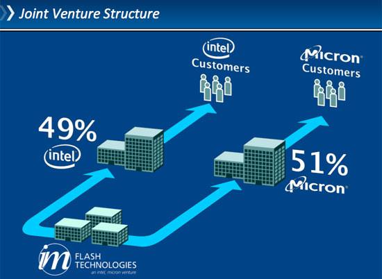
Intel and Micron jointly formed IMFT (Intel-Micron Flash Technologies), LLC back in 2006. The two companies share production from the venture. Intel gets 49% of IMFT’s flash production and Micron gets 51%.
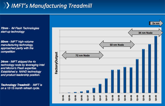
In the usual Intel tradition, IMFT aggressively scales process technology to be competitive. The company started manufacturing at 72nm, spent 2008 at 50nm and just last year scaled down to 34nm. The latter is what found its way into Intel’s X25-M G2 as well as Micron’s soon-to-be released RealSSD C300.
Today IMFT is announcing that it has begun sampling 2-bits-per-cell MLC NAND flash manufactured using 25nm transistors. The company believed it had a 6 month head start over the competition in 34nm, and now believes that with 25nm NAND it’s roughly a year ahead of anyone else.
Volume production will happen sometime in Q2, with products shipping before the end of the year. In my last SSD article I mentioned that Intel’s 3rd generation X25-M would be shipping in Q4 at 160GB, 320GB and 600GB. These drives will use IMFT’s new 25nm flash.
The first 25nm product is an 8GB (64Gbit) 2-bits-per-cell MLC NAND flash. A single 8GB die built on IMFT’s 25nm process has a die size of 167mm2. Immersion lithography is apparently necessary to produce these 25nm NAND devices, but the extent is unclear. This is technically Intel’s first device that requires immersion lithography to manufacture.
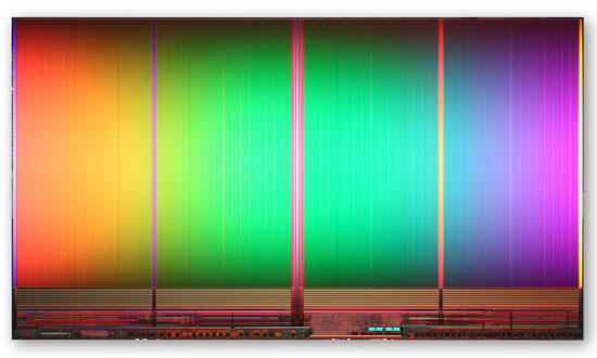
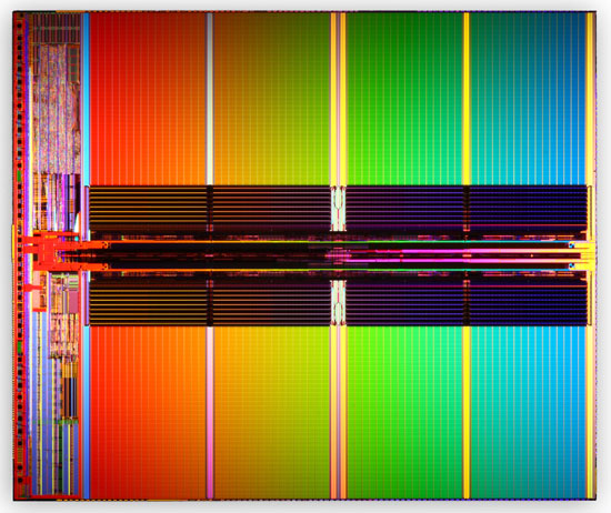
25nm IMFT 2-bit MLC NAND Flash, 8GB, 167mm2
The 34nm flagship was a 4GB (32Gbit) 2-bits-per-cell MLC NAND device with a die size of 172mm2. At 25nm you basically get twice the capacity at the same die size, which should translate into twice the SSD capacity at the same price as a 34nm drive today.
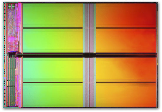
34nm IMFT2-bit MLC NAND Flash, 4GB, 172mm2
Obviously supply and demand economics play their roles here. We may not see the sort of aggressive pricing we want to on 25nm X25-M drives if demand remains as high as it has been for the 34nm G2s.
Last year IMFT announced plans to deliver a 3-bit-per-cell 34nm MLC NAND flash. Today's announcement pretty much negates the need to bring those devices to market. Although at some point we'll probably see 3-bit-per-cell at 25nm. At this point 3-bit-per-cell MLC flash is only suitable for cheaper or low cycle devices like USB sticks. In a SSD the performance and reliability tradeoffs just aren't worth it.
34nm IMFT 3-bit MLC NAND Flash, 4GB, 126mm2
The 25nm IMFT NAND devices support ONFi 2.2, meaning the interface speed can reach a maximum of 200MB/s.
The other major change to the 25nm NAND is an increase in the page size. At 50nm and 34nm, IMFT’s page size was 4KB. At 25nm on the 8GB device the page size is now 8KB. Block size has also gone up from 128 pages to 256 pages. This will obviously have performance implications and require some firmware reorganization, but given that Intel has known this was coming for some time now I would expect that its 3rd generation drives will be optimized for 25nm.
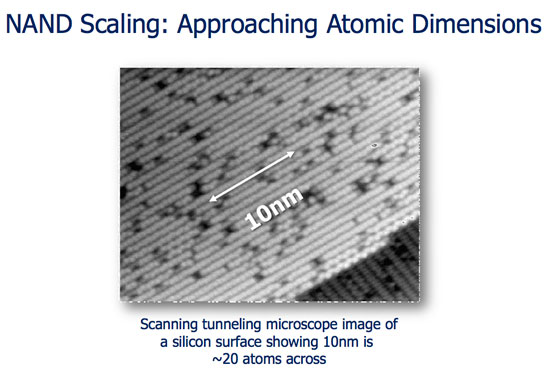
IMFT believes there’s still hope for scaling flash devices even further. It's ridiculous to think about how small these transistors are getting. As we approach single-digit-nm dimensions we can start counting atoms when we look at these transistors:
Right now IMFT is on a 12 - 15 month cycle, so we can expect the next process shrink to begin sampling in mid-2011, shipping in 2012.
If IMFT can ramp up production of 25nm NAND flash, 2012 may be the year of the first truly affordable mainstream SSDs.


39 Comments
View All Comments
semo - Monday, February 1, 2010 - link
of course it needs an overhaul but it won't happen. we'll be talking about LBAs in 20 years time. Just like x86chemist1 - Saturday, January 30, 2010 - link
I'd like to see someone manufacture one of these super-fast SSDs in a PCI ExpressCard/34 format, which would fit flush into the PCI slot on my MacBook Pro. [See http://www.macworld.com/article/145185/2009/12/mbp...">http://www.macworld.com/article/145185/2009/12/mbp...]Since mine is an early-2008 model, it can't take full advantage of SATA-connected SSDs, being limited to 150 MB/sec on the SATA interface (and Apple shows no signs of upgrading the firmware). By contrast, PCI Express Cards are 2.5 Gb/sec, which is about 310 MB/sec. This would also effectively give me two drives, leaving the HD for mass storage.
FileMate does make some ExpressCard SSDs. However, while faster than a conventional HD, they are significantly slower than the current Intel SSDs.
ksherman - Sunday, January 31, 2010 - link
just swap out your DVD drive for another hard drive. I got an Intel 80GB in place of my DVD drive and a 500GB Seagate in the main drive bay. Though, I hardly ever used my DVD drive.chemist1 - Sunday, January 31, 2010 - link
Thought of that, but it voids the remaining 2 years on my extended warranty (yes, it's an early 2008 model, but I purchased it in Feb. 2009 on clearance). And I do actually use the DVD drive with some frequency.milli - Saturday, January 30, 2010 - link
Toshiba already has 3-bits-per-cell & 4-bits-per-cell MLC NAND.ioannis - Saturday, January 30, 2010 - link
that is all nice and good, but is there any news on memristors? I know it's HP and not Micon/Intel working on those, but just wondering...jwilliams4200 - Saturday, January 30, 2010 - link
Anand:Do you know how many NAND die can be assembled in each package?
I remember seeing the circuit board of the 160GB G2, and it looked liked it only had 10 NAND packages (unless they were double-stacked?) So that would be 16GB per package, or 4 of the 32 Gbit die per package.
But the 80GB G2 also has 10 packages, I think (at least, the controller is 10 channel). So is it using only 2 die per package?
Can more than 4 die be assembled in each package? Having, say, 8 of the upcoming 64 Gbit die in a package blows my mind.
PandaBear - Saturday, January 30, 2010 - link
Toshiba have done 16 dies, but the yield is very low, the economy of scale stop at 4 die per chip.AnandMeat - Saturday, January 30, 2010 - link
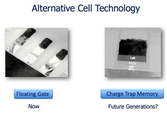
Anand,I thought a floating gate device was technically a charge trapping device since it involves some kind of charge transfer and holding in the electrically isolated floating gate. Is the only difference between a "charge trapping" device and a floating gate device something like the floating gate being made of a nitride? Or is all this just bad nomenclature? Thanks!
Meat
PandaBear - Saturday, January 30, 2010 - link
They are the same thing. All charge trapping devices like EEPROM, NOR, and NAND uses floating gate and it is how you arrange them that makes the difference.