At this year’s Consumer Electronics Show, NVIDIA had several things going on. In a public press conference they announced 3D Vision Surround and Tegra 2, while on the showfloor they had products o’plenty, including a GF100 setup showcasing 3D Vision Surround.
But if you’re here, then what you’re most interested in is what wasn’t talked about in public, and that was GF100. With the Fermi-based GF100 GPU finally in full production, NVIDIA was ready to talk to the press about the rest of GF100, and at the tail-end of CES we got our first look at GF100’s gaming abilities, along with a hands-on look at some unknown GF100 products in action. The message NVIDIA was trying to send: GF100 is going to be here soon, and it’s going to be fast.
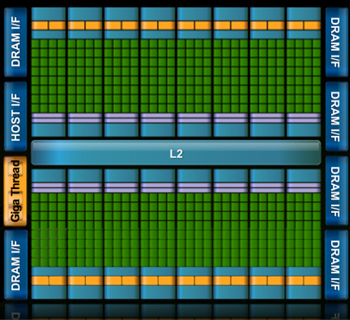
Fermi/GF100 as announced in September of 2009
Before we get too far ahead of ourselves though, let’s talk about what we know and what we don’t know.
During CES, NVIDIA held deep dive sessions for the hardware press. At these deep dives, NVIDIA focused on 3 things: Discussing GF100’s architecture as is relevant for a gaming/consumer GPU, discussing their developer relations program (including the infamous Batman: Arkham Asylum anti-aliasing situation), and finally demonstrating GF100 in action on some games and some productivity applications.
Many of you have likely already seen the demos, as videos of what we saw have already been on YouTube for a few days now. What you haven’t seen and what we’ll be focusing on today, is what we’ve learned about GF100 as a gaming GPU. We now know everything about what makes GF100 tick, and we’re going to share it all with you.
With that said, while NVIDIA is showing off GF100, they aren’t showing off the final products. As such we can talk about the GPU, but we don’t know anything about the final cards. All of that will be announced at a later time – and no, we don’t know that either. In short, here’s what we still don’t know and will not be able to cover today:
- Die size
- What cards will be made from the GF100
- Clock speeds
- Power usage (we only know that it’s more than GT200)
- Pricing
- Performance
At this point the final products and pricing are going to heavily depend on what the final GF100 chips are like. The clockspeeds NVIDIA can get away with will determine power usage and performance, and by extension of that, pricing. Make no mistake though, NVIDIA is clearly aiming to be faster than AMD’s Radeon HD 5870, so form your expectations accordingly.
For performance in particular, we have seen one benchmark: Far Cry 2, running the Ranch Small demo, with NVIDIA running it on both their unnamed GF100 card and a GTX285. The GF100 card was faster (84fps vs. 50fps), but as Ranch Small is a semi-randomized benchmark (certain objects are in some runs and not others) and we’ve seen Far Cry 2 to be CPU-limited in other situations, we don’t put much faith in this specific benchmark. When it comes to performance, we’re content to wait until we can test GF100 cards ourselves.
With that out of the way, let’s get started on GF100.


115 Comments
View All Comments
Stas - Tuesday, January 19, 2010 - link
all that hype just sounds awful for nVidia. I hope they don't leave us for good. I like AMD but I like competition more :)SmCaudata - Monday, January 18, 2010 - link
The 50% larger die size will kill them. Even if the reports of lower yields are false they will have to get a much smaller profit margin on their cards than AMD to stay competetive. As it is the 5870 can run nearly any game on a 30" monitor with everything turned up at a playable rate. The target audience for anything more than a 5870 is absurdly small. If Nvidia does not release a mainstream card the only people that are going to buy this beast are the people that have been looking for a reason not to buy and AMD card all along.In the end I think Nvidia will loose even more market share this generation. Across the board AMD is the fastest card at every price point. That will not change and with the dual GPU card already out from ATI it will be a long time before Nvidia has the highest performing card because I doubt they will release a dual GPU card at launch if they are having thermal issues with a single GPU card.
BTW... I've only ever owned Nvidia cards but that will likely change at my next system build even after this "information."
Yojimbo - Monday, January 18, 2010 - link
what do you mean by "information"?SmCaudata - Monday, January 18, 2010 - link
Heh. Just that it was hyped up so much and we really didn't get much other than some architectural changes. I suppose that maybe this is really interesting to some, but I've seen a lot of hardware underperform early spec based guesses.The Anandtech article was great. The information revealed by Nvidia was just okay.
qwertymac93 - Monday, January 18, 2010 - link
I really hope fermi doesn't turn into "nvidias 2900xt". late, hot, and expensive. while i doubt it will be slow by any stretch of the imagination, i hope it isn't TOO hot and heavy to be feasible. i like amd, but nvidia failing is not good for anybody. higher prices(as we've seen) and slower advancements in technology hurt EVERYONE.alvin3486 - Monday, January 18, 2010 - link
Nvidia GF100 pulls 280W and is unmanufacturable , details it wont talk about publiclyswaaye - Monday, January 18, 2010 - link
Remember that they talked all about how wondrous NV30 was going to be too. This is marketing folks. They can have the most amazing eye popping theoretical paper specs in the universe, but if it can't be turned into something affordable and highly competitive, it simply doesn't matter.Put another way, they haven't been delaying it because it's so awesome the world isn't ready for it. Look deeper. :D
blowfish - Monday, January 18, 2010 - link
This was a great read, but it made my head hurt!I wonder how it will scale, since the bulk of the market is for more mainstream cards. (the article mentioned lesser derivatives having less polymorph engines)
Can't wait to see reviews of actual hardware.
Zool - Monday, January 18, 2010 - link
Iam still curious why is nvidia pushing this geometry so hard. With 850 Mhz the cypress should be able to make 850mil polygons/s with one triangel/clock speed. Now thats 14 mil per single frame max at 60fps which is quite unrealistic. Thats more than 7 triangels per single pixel in 1920*1050. Making that amount of geometry in single pixel is quite waste and also botlenecks performance. U just wont see the diference.Thats why amd/ati is pushing also adaptive tesselation which can reduce the tesselation level with copute shader lod to fit a reasonable amount of triangels per pixel.
I can push teselation factor to 14 in the dx9 ATI tesselation sdk demo and reach 100fps or put it on 3 and reach 700+ fps with almost zero difference.
Zool - Tuesday, January 19, 2010 - link
Also want to note that just tesselation is not enough and u always use displacement mapping too. Not to mention u change the whole rendering scene to more shader demanding(shadows,lightning) so to much tesselation (like in uniengine heaven on almost everything, when without tesselation even stairs are flat) can realy make big shader hit.If u compare the graphic quality before tesselation and after in uniengine heaven i would rather ask what the hell is taken away that much performance without tesselation as everything looks so flat like in a 10y old engine.
The increased geometry setup should bring litle to no performance advantage for gf100, the main fps push are the much more eficience shaders with new cache architecture and the more than double the shaders of course.